This page belongs to a series of pages about timing. The previous pages explained the theory behind timing calculations, showed how to write several timing constraints and discussed the principles of timing closure. This page starts the discussion about I/O timing constraints.
Introduction
Until this point, the entire discussion about timing constraints has related to paths that are inside the FPGA. It's finally time to talk about the constraints that control the timing of the FPGA's I/O ports.
But before talking about the timing constraints, it's necessary to be aware of the different methods to synchronize between the FPGA and the external component. Timing constraints that are written without considering this topic may be worthless. Furthermore, the logic that is responsible for the I/O interface may be written inadequately. In extreme cases, the PCB may lack the necessary wiring to allow for I/O that is guaranteed to work.
With the required awareness of the synchronization with the external component, it's possible to choose the correct commands for timing constraints. The practical aspects for that are explained on the next page.
On this page, I assume that you're acquainted with IOB registers.
Clock distribution
As long as the paths were inside the FPGA, there was no need to be aware of the clock skew between the two sides of the path: The tools were responsible for the distribution of the clock, and the timing calculations took the clock skew into account.
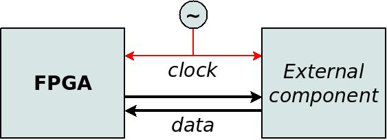
With I/O timing constraints, it's different: One side of the path is an external component outside the FPGA. In order to synchronize with the data signals, this component relies on a clock that it receives on one of its pins. But what is this clock synchronized with?
The strategy is usually one of these two:
- System synchronous clock: The external component is connected to the same clock signal as the FPGA's clock input pin. This strategy is also called common clock.
- Source-synchronous clock: A special clock signal is supplied together with the data signals. Usually the data signals change value simultaneously with the clock: Either with the rising edge or with the falling edge.
These two strategies are discussed in more detail next. Regarding the source-synchronous clock option, there is a significant difference if the data signals are inputs and outputs. These scenarios are hence discussed separately.
System synchronous clock
The simplest method for synchronizing several components on a PCB is to connect all components to one clock. This is called system synchronous clock (or common clock).
The advantage of this method is that the timing parameters of all components are relative to one clock signal. Hence the clock is the same on both sides for the sake of making timing calculations. So for a data signal that propagates between two components on the PCB, the calculation is similar to a path inside the FPGA: The path begins with a clock-to-output that is relative to the first clock edge. At the path's end, the tsu is relative to the second clock edge. The system synchronous method means that these two clock edges belong to the same clock.
So working with a system synchronous clock is simple, however this method is suitable only for relatively low frequencies. Recall from the introduction on timing calculations that the minimal clock period is the sum of several timing parameters: The clock-to-output of the first flip-flop, the propagation delay and the tsu of the second flip-flop. For an output port, the clock-to-output is relatively large, because this is the amount of time that it takes the PCB's wire to reach the required voltage. But it doesn't end with that: The clock skew and other uncertainties that are related to the clock must be added too. With all numbers summed up, the minimal clock period may not be impressive.
As a rule of thumb, a system synchronous clock is not suitable for I/O with a data rate that is higher than 100 MHz. But this depends a lot on which components are involved. In fact, some electronic components have timing requirements that are very difficult to satisfy with a system synchronous clock, even at much lower frequencies. Such components are one of the reasons why it's important to plan the I/O timing before manufacturing the PCB.
set_input_delay and set_output_delay (which are explained on the next page) are the most suitable timing constraints for use together with a system synchronous clock.
Source-synchronous clock
Quite often, the interface between two components on a PCB is based upon a clock that is supplied by one of these components. Naturally, it makes a difference if the clock is generated by the FPGA or the external component.
There are hence four relevant scenarios:
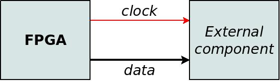
- The data and the clock are outputs that are generated by the FPGA. This relatively easy scenario is discussed separately on the page about source-synchronous outputs.
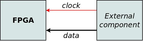
- The data and the clock are generated by the external component. Hence the FPGA receives these as input signals. A page about source-synchronous inputs is dedicated to this scenario.
- The clock is generated by the FPGA, but the data is bidirectional (or inputs). This is a special case of source-synchronous inputs. The fact that the FPGA generates the clock doesn't make a big difference: The data inputs are synchronized with the clock on the PCB. This clock has a delay in relation to the clock inside the FPGA. See the page about source-synchronous outputs for more about this scenario.
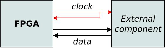
- The clock is generated by the external component, and the data is bidirectional. Regarding the inputs to the FPGA, this is similar to the scenario where the data is generated by the external component (source-synchronous clock). As for the FPGA's outputs, they behave like any output that is synchronous with an external clock. Hence these outputs are arranged as if they were system synchronous.
Asynchronous inputs
Some inputs are not associated with a clock. For example, pushbuttons, I2C, RS232 and various status signals from external components are not synchronized with a clock. These signals are usually much slower than the clock inside the FPGA. The usual solution is therefore to sample these signals with flip-flops (preferably IOB registers) and continue with regular logic design techniques.
These inputs are not synchronized with the clock that is used for sampling. Therefore, the IOB register (or the flip-flop that is connected to the port) fulfills the role of a metastability guards. A second register should therefore be used for each port, similar to a clock domain crossing between unrelated clocks. Otherwise, there is a risk for unpredictable and weird behavior, even if the input signals are slow and the design seems to work properly at the moment.
The timing constraints should be written to ensure repeatable behavior: The same guidelines as for IOB registers should be followed, even if the flip-flops are not placed inside the IOB. To be extra safe, it's a good idea to also add a dedicated timing constraint in relation to these registers' role as metastability guards (this is explained on a different page).
False paths
False paths for I/O ports are in principle the same as for paths inside the FPGA: The set_false_path command is used to request that no timing requirements are enforced for specific ports.
False paths have already been discussed regarding paths that are inside the FPGA. Based upon the same rationale, the motivation behind false paths for I/O ports is mainly to maintain an empty list of unconstrained paths. This list should be empty in order to make it easier to identify when a port lacks timing constraints due to a mistake.
False paths should be used only when the timing of the port is completely meaningless. For example, with LEDs and DIP switches.
Examples of SDC constraints:
set_false_path -to [get_ports led_0]
set_false_path -from [get_ports dip_switch_0]
Summary
This page has outlined a few strategies for synchronizing between the FPGA and the external component. The selected strategy has an influence on the logic design as well as the timing constraints.
With this knowledge, it's time to discuss how to write the I/O timing constraints.