This page belongs to a series of pages about timing.
About this page
It's impossible to get the timing done correctly without knowing a few basic topics in logic design. This page explains a few fundamental concepts, which are the basis for the rest of this series of pages.
Everything that is written below is taught in academic courses about logic design. However, not everyone who works with FPGAs have taken a course of this sort, and even those who have taken such course don't necessarily remember everything. This page is intended to fill the missing parts, if such exist.
Feel free to skip the parts on this page that you already know, but it's still recommended to read through everything, even if this reading is superficial. The last sections on this page are in particular important for understanding the next pages in this series.
A brief review
Before getting into the concepts that relate to timing, I shall make a quick review of some relevant terms in logic design. If any of these terms isn't known already, I suggest making yourself familiar with it before continuing on this page.
First, combinatorial logic. This term is used to describe elements such as logic gates: AND gate, OR gate, NOT gate, etc. These logic elements are considered combinatorial logic because they have no memory. In other words, their behavior doesn't depend on what has happened in the past. The value at the output of these logic elements depends only on the values at the inputs.
An important type of combinatorial logic is the look-up table (LUT). This is a multi-purpose logic element, which implements any logic function that depends on a number of inputs. The LUT is important because it is used for almost all combinatorial logic inside an FPGA. The LUTs inside an FPGA are implemented as asynchronous ROMs (i.e. ROMs without a clock): The inputs are treated the address to the data inside the LUT. The output usually consists of one or two bits.
The number of inputs to these LUTs is 4 or 6 in almost all FPGAs in the market, so the number of memory cells in each LUT is either 16 or 64.
The next important term is sequential logic. This includes flip-flops, synchronous RAMs, and many other building blocks that require a clock in order to operate. All these logic elements become active as a reaction to a specific change of the clock. Between these moments of activity, sequential elements ignore their inputs, retain their internal state, and don't change their outputs.
For example, positive edge triggered logic elements are active when the clock changes from low to high, i.e. a rising clock edge. Likewise, negative edge triggered logic elements are active when the clock changes from high to low, i.e. a falling clock edge. There are also logic elements that are active on both clock edges, but such logic elements are used almost only for sampling I/O signals or producing them.
All sequential elements have some kind of memory. This is an immediate conclusion from the fact that they don't change their output until a clock edge arrives. Some sequential elements have the minimal amount of memory, which is exactly one bit of memory for each output. Other sequential elements have more memory, for example shift registers and RAMs.
For the sake of discussing timing, there are only two important facts: The input is sampled only in conjunction with a clock edge, and the output changes almost only as a result of a clock edge. There is only one exception, which is that some sequential elements have an asynchronous reset input. When this input is active (high or low, depending on the logic element), the internal state of the sequential element changes to a predefined value immediately, regardless of the clock. As a result, some or all outputs of this element also change immediately to a known value.
In an FPGA, some sequential elements have an asynchronous reset, and others don't. The asynchronous reset is the only asynchronous input that is possible in almost all sequential elements on an FPGA. This is even though the theory of logic design includes several elements with multiple asynchronous inputs, e.g. the S-R flip-flop.
From now on, I'll talk about flip-flops
For the sake of simplicity, I shall assume that all sequential elements are positive edge triggered flip-flops, i.e. flip-flops that are active in reaction to a rising edge of the clock. In other words, all sequential elements are will be represented here with flip-flops. These flip-flops respond to their inputs and update their outputs only when the clock changes from low to high.
It's easier to understand timing this way, and the discussion about the flip-flop is easily generalized to any other sequential element.
Setup and hold
In order to ensure that a flip-flop operates correctly and reliably, its inputs must be stable (i.e. not change its value) according to two timing requirements:
- The input must be stable during a period of time before the clock edge. This amount of time is called the setup time, and is marked tsu.
- The input must be stable during a period of time after the clock's edge. This amount of time is called the hold time, and is marked thold.
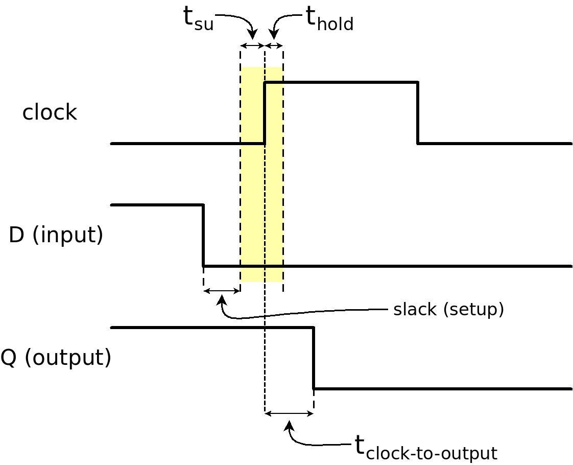
The drawing above shows the meaning of tsu and thold: The D input is not allowed to change value inside the time period that is marked with yellow. In this example, D changes from high to low with legal timing, i.e. outside this yellow time period.
One way to understand these two timing parameters is like this: It's quite obvious, that if an input to a flip-flop changes exactly together with the clock edge, it's unclear if the flip-flop will treat that input as high or low. What should it choose? The state just before the clock edge or after it?
Then we can ask what it means that the input changed "exactly together" with the clock edge. How exact is that? The two timing parameters, tsu and thold define how far from the clock edge it is safe to change the input's value. These parameters are defined for all sequential elements with the same meaning.
It's important to note that if this timing requirement is violated, the consequence can be much worse than just that the output of the flip-flop after the clock edge is random. These are the two main reasons for that:
- In some cases, the FPGA tools automatically duplicate flip-flops of the logic design during the implementation of the project, in particular to reduce fan-out. By doing so, part of the logic that depends on this flip-flop's value is connected to one flip-flop, and another part of the logic is connected to the second flip-flop. This is OK as long as both flip-flops have the same output all the time. But if the timing requirements (tsu and thold) are violated, each of these two flip-flops can have a different value at their outputs.
- A flip-flop can fall into a state of metastability if the timing requirements are violated. In this state, the output of the flip-flop is neither high or low for a short while. More on metastability and its adverse consequences can be found on this page.
Clock-to-output
The third timing parameter that is defined for all sequential elements is the clock-to-output time, which has several common symbols, e.g. tcko, tco, tC_Q etc. This parameter is not a timing requirement. Rather, this parameter says when the output (Q) of the sequential element is guaranteed to be valid. More precisely, how much time after the clock edge the output is valid (see the timing diagram above).
In fact, there are two parameters on this matter:
- The maximal clock-to-output: How much time it takes until the output is valid after a clock edge.
- The minimal clock-to-output: How much time the output is guaranteed to remain unchanged after a clock edge.
Most of the time, only the maximal clock-to-output is interesting, so when this parameter is given in a datasheet it's almost certainly the maximal value.
Note that if the flip-flop's timing requirements (tsu and thold) are violated, there is no guarantee on when the output is stable. In this case, the maximal clock-to-output parameter is meaningless because of the possibility that the flip-flop remains in an undefined state (metastability) for a short while.
tsu and thold can be negative
Even though the drawing above shows positive tsu and thold, it's possible that one of these parameters has a negative value. In fact, this happens often with flip-flops inside FPGAs.
For example, a negative tsu means that the data doesn't have to be stable when the clock edge arrives. Rather, the data must have reached its stable value slightly after the clock edge. But tsu still puts a limit on how much after the clock edge.
Likewise, a negative thold allows the data to change before the clock edge. Once again, there is still a limitation to how much before this is allowed, and this is reflected by thold.
However, because tsu and thold can be negative, it's theoretically possible to define timing requirements that are nonsense.
To explain this, denote tsamp as the actual time that the flip-flop samples its input. tsamp isn't known in advance, but the definition of tsu tells us that –tsu < tsamp. In other words, the flip-flop samples its input after the data has stabilized following a change, which is what tsu ensures. By the same principle, tsamp < thold: The sampling must occur before the data can change in response to a clock edge. Putting these two together, we have –tsu < tsamp < thold, or simply –tsu < thold. This must be true for any pair of tsu and thold.
So tsu or thold can be negative as long as they meet this condition. But both can't be negative at the same time.
The clock-to-output parameter is always positive: A flip-flop can't possibly react to a clock edge before it has arrived. By contrast, note that the fact that tsamp can be negative doesn't imply that sampling took place before the clock edge. Rather, this can happen due to a delay of the data signal.
Propagation delay
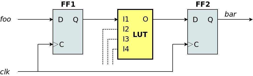
The drawing above shows a simple connection between two flip-flops with a LUT in the middle. For the sake of simplicity, let's assume that the LUT's output depends only on I1. For example, this logic could be the result of the following Verilog code, so the LUT implements a NOT gate:
always @(posedge clk)
  begin
    foo_reg <= foo;   // FF1 = foo_reg
    bar <= !foo_reg;  // FF2 = bar
  end
Note that both flip-flops are connected to the same clock. What is this clock's maximal frequency?
To answer this question, there's a missing piece of information: How much time does it take from the moment that FF1's output has a stable value until FF2's input has a stable value? We shall mark with time as tpd (propagation delay).
Note that the term propagation delay always relates to a specific segment of combinatorial logic. It's important to explicitly define which segment it relates to. For example, it's also possible to define the time from the LUT's I1 to the same LUT's O (from its input to output) as a propagation delay. This delay is probably different from the previous definition of tpd.
In particular, on an FPGA, there is a routing delay between the output of FF1 and the input of the LUT. So in real life, FF1's Q is not the same point as the LUT's I1, and it takes some time for the signal to propagate between these two points.
Because of this ambiguity, it's rare to see the symbol tpd in datasheets for FPGAs. And when a propagation delay is given in such datasheets, the accurate meaning of this parameter is usually written explicitly.
I'll get back to the clock's maximal frequency later.
The path
It's difficult to give a concise definition of a path, but we have already seen an example for it. Above, I defined tpd as the propagation delay between FF1's Q and FF2's D. This tpd relates to a specific scenario: FF1 changes its value, and then the updated value reaches the LUT, after which the LUT changes its output, and finally the updated value reaches FF2. This sequence of events starts by the change of only one signal (FF1's output), and ends when the signal at a different point (FF2's input) is stable.
So tpd is defined as the propagation delay of the path from FF1's Q to FF2's D. Or for short, the path from FF1 to FF2.
The path consists of all elements that cause a delay from the beginning of this sequence to its end. There are two types of elements in the path:
- Elements of combinatorial logic, which contribute to the delay because it takes some time until the electronic circuits update the signals at their outputs. This is often referred to as logic delay. In the example above, the LUT is the element of this sort.
- Routing. This is just the wires between the logic elements. These segments contribute to the delay because it takes time for a signal to move through space, and also because a change of voltage involves charging capacitors along the way.
The purpose of a path is to calculate its propagation delay. How the result of this calculation is used is shown next.
Often a path represents a theoretic experiment where one flip-flop's output changes, and we follow a specific route that leads to the input of another flip-flop. In this theoretic experiment, an imaginary stopwatch is started when the output of the first flip-flop changes. When the input of the second flip-flop changes, this stopwatch is stopped.
This theoretic experiment helps answering whether the time that this stopwatch shows is too long, which means that the requirement for tsu has been violated. A second question is whether this time is too short, so thold has been violated.
Note that the route of a path includes only wiring and combinatorial logic. Hence the time it takes until the signal is stable at the destination depends only on the elements of combinatorial logic and the routing along the path. It doesn't matter when this theoretic experiment is made, the result is always the same.
In a real FPGA design, each flip-flop usually has many paths that reach its input, and many paths that begin at its output. In fact there can be more than one path between a pair of flip-flops as well. And yet, the timing calculations are always made with the assumption that only one flip-flop has changed its output, and everything that happens in the FPGA's logic is a direct result of that change. The number of paths that are calculated in an FPGA design can be enormous, but this is of course done automatically by the software.
A simple static timing analysis
For the sake of demonstration, I'll make a simple timing analysis of the example above with two flip-flops. The topic of timing constraints will be discussed later, but for the time being, let's assume that @clk has a frequency of 250 MHz (4 ns), and that it's connected directly to the logic (i.e. without a PLL, which is not recommended in a real design, but this simplifies the timing analysis). The timing constraint (in SDC style) could be something like this:
create_clock -period 4.000 -name clk [get_ports clk]
An example of a real timing analysis is shown on the next page in this series, but that analysis is accurate, and therefore contains a lot of details that makes it difficult to understand. So this is a simple analysis, which just demonstrates the principle.
The analysis performs the theoretic experiment that was mentioned above: An imaginary stopwatch starts together with @clk's rising edge. This is the chain of events, along with the (fictitious) delay that each event contributes.
- Clock-to-output of FF1 (0.2 ns): The time it takes before FF1's output (Q) is updated with the value at the flip-flop's input (D).
- Routing delay to I1 (0.3 ns): The time it takes for the signal to travel from FF1's output to the LUT's input (I1).
- The LUT's propagation delay (0.3 ns): The LUT needs this time to update its output (O) after any of its inputs (I1 in this case) has changed.
- Routing delay to FF2's input (0.4 ns): The time it takes for the signal to travel from the LUT's output to FF2's input (D)
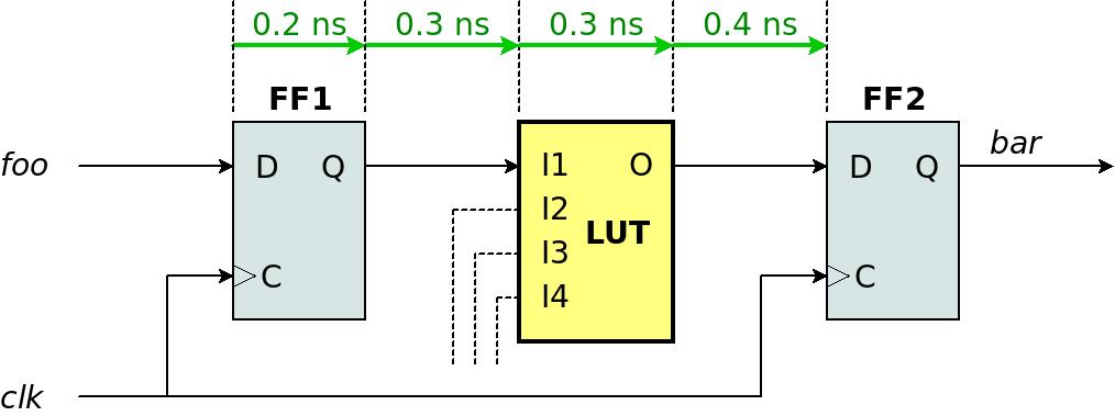
The propagation delay (tpd) of this path is the sum of all these delays: 0.2 + 0.3 + 0.3 + 0.4 = 1.2 ns. For the sake of the example, let's suppose that FF2's tsu is 0.1 ns. This means that FF2's input (D) must be stable 0.1 ns before the next rising edge of @clk. In other words, the maximal tpd that is allowed is 4 - 0.1 = 3.9 ns.
But tpd is just 1.2 ns, so according to this calculation, the path achieves the timing constraint with a large margin. This margin is called slack, and in this case it's 3.9 - 1.2 = 2.7 ns. When this number appears in the software's timing calculations, it indicates if the tools had a hard time to achieve the timing constraints or not: If the slack is close to zero, it often indicates that the software had to work hard to make the path meet the timing requirements.
The propagation delay also allows us to calculate the maximal frequency of @clk that this path can achieve timing with. tpd is 1.2 ns, and the tsu requirement means that next rising edge can arrive 0.1 ns later. In other words, there must be at least 1.3 ns between the rising edges. That means a frequency of about 769 MHz. This is a very high frequency, but it's a realistic result because the path contains just a single LUT. Real-life logic is usually more complicated than so, which is why real-life frequencies are often much lower.
A real static timing analysis makes this calculation exactly, but it's only part of the story. The path that was calculated here is called the data path in a real calculation. However, a real static timing analysis also takes into consideration that the clock edge doesn't arrive to both flip-flops at the exact same time. This is because the delay from the clock buffer to each of these flip-flops is slightly different. This difference between these delays is called clock skew. Also, the time between each clock edge isn't exactly the same because of clock jitter. These issues with the clock make the accurate calculation more complicated, as shown on the next page.
Recovery and Removal
If a flip-flop has an asynchronous reset input (are you sure you want that?), there are requirements on when this input becomes inactive. Note that it doesn't matter when the reset becomes active, because the flip-flop will change to a known state anyhow.
But when the reset becomes inactive, the flip-flop starts to be sensitive to the clock. If this deactivation of the reset occurs close to a clock edge, it's not clear if the flip-flop should respond to it. Just like tsetup and thold, the reset must be stable during a time period around the clock edge. Or, more specifically:
- The reset must not change from active to inactive during a period of time before the clock edge. This amount of time is called the recovery time. This is the time it takes for the flip-flop to recover from the reset and become ready for a clock edge.
- The reset must not change from active to inactive during a period of time after the clock's edge. This amount of time is called the removal time.
These definitions are similar to those of tsetup and thold. That is not a coincidence: The recovery time is a special kind of a setup time. The timing analysis is done the same way. The only difference is that the setup time is relevant regardless of the value of the data signal. By contrast, the recovery time is not enforced when the asynchronous reset signal changes to active. The relation between the removal time and the hold time is the same.
Because of this similarity, Recovery and Removal will not be discussed beyond this mention. Also note that the said above is true for all asynchronous inputs, not just asynchronous reset.
The RTL paradigm and timing
The example with two flip-flops that was shown above is simple, but it represents all logic that is created with the RTL paradigm: Each path begins at a flip-flop and ends at a flip-flop with the same clock (or a related clock). The path itself consists of combinatorial logic and routing. In this example, the combinatorial logic is just one LUT, but there is no substantial difference between this and several logic elements in the path. The structure is the same.
The reason that the RTL paradigm is so important is that when this method is used, almost all data paths have this same simple structure. And because the number of paths in a logic design is often huge, the simplicity of the timing analysis helps preventing mistakes. Among others, the fact that the timing analysis has a specific pattern makes it possible to read the timing report and ask if it makes sense.
So to the extent possible, everything should start at a sequential element and end at a sequential element. This is a useful guideline when writing Verilog code as well as when planning the logic's structure in general.
This concludes the brief introduction to the theory behind timing constraints. A clock period constraint and the related timing reports are explained on the next page.