Introduction
This page discusses source-synchronous data outputs. This technique means that the data outputs are synchronous with a clock that the FPGA generates in parallel with these outputs.
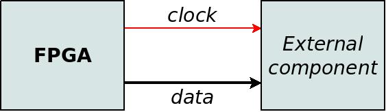
This approach is the obvious choice if the interface with an external component consists of only output ports from the FPGA. It is also suitable if the I/O is bidirectional, as discussed at the bottom of this page. There is also a separate page that discusses the relations between clock and data in general.
The basic application
Consider this Verilog example:
module top (
   input clk,
   output reg [7:0] data_out,
   output reg sync_clk_out
);

   always @(posedge clk)
     begin
	sync_clk_out <= !sync_clk_out;
	if (sync_clk_out)
	  data_out <= data_out + 1;
     end
endmodule
Note that @data_out changes its value simultaneously with @sync_clk_out's falling edge: When @sync_clk_out is low, @data_out doesn't change. When @sync_clk_out is high, @data_out changes to a new value in response to @clk's rising edge.
If IOB registers are used for both @data_out and @sync_clk_out, all of these output signals change their value at practically the same time. The external component that receives these signals can therefore use @sync_clk_out as its clock. It's usually easy to meet the external component's timing requirements this way (assuming that the sampling of @data_out is synchronized with @sync_clk_out's rising edge).
Using DDR registers
The example above has a significant drawback: The frequency of @sync_clk_out is half the frequency of @clk. Hence the data rate of @data_out is limited to half the frequency of @clk as well. The only exception is if the external component is sensitive to @sync_clk_out's both clock edges (i.e. it has a DDR input). This is usually not the case.
It's possible to use an output DDR register in order to generate an output clock that is aligned with the data outputs. The idea is to use a flip-flop that changes its value on both clock edges. Hence such a flip-flop behaves like this:
   always @(posedge clk or negedge clk)
     if (clk)
       sync_clk_out <= 0;
     else
       sync_clk_out <= 1;
@sync_clk_out changes to low in response the rising edge of @clk. The opposite happens due to a falling edge. The result is an output clock with the same frequency.
However, this Verilog code will not work with most synthesizers, because the flip-flops in the logic fabric are usually not capable of being sensitive to both clock edges. Only IOB registers have this capability, and the synthesizer is rarely clever enough to comprehend this possibility.
Therefore, an instantiation of a logic primitive is required. The primitive is specific to the FPGA that is used. This example shows how this can be done for Kintex Ultrascale:
   ODDRE1 ODDR_ins
     (.C(clk), .Q(sync_clk_out),
      .D1(1'b0), .D2(1'b1),
      .SR(1'b0));
But now the clock is generated with an output DDR register and the data signals are generated with regular IOB registers. The alignment between the data and clock is not as obvious as it was before. It's therefore important to read the timing reports for all outputs, and verify that the difference between the delays is small enough.
It's also possible to use output DDR registers for the data as well: If the same value is given to D1 and D2, the output changes only once for each clock cycle:
module top (
   input clk,
   output [7:0] data_out,
   output sync_clk_out
);

   reg [7:0]  data;

   ODDRE1 ODDR_ins
     (.C(clk), .Q(sync_clk_out),
      .D1(1'b0), .D2(1'b1),
      .SR(1'b0));

   ODDRE1 ODDR_data_ins [7:0]
     (.C(clk), .Q(data_out),
      .D1(data), .D2(data),
      .SR(1'b0));

   always @(posedge clk)
     data <= data + 1;
endmodule
This method ensures that the data and clock is aligned. The explicit instantiation of the output DDR registers also ensures that IOB registers are used. The only drawback with this method is that it is specific to each FPGA.
Note that the behavior of output DDR registers can be unexpected and confusing. For example, note that @data is synchronized with the positive edge of @clk. But the ODDRE1 is active on both clock edges. Be sure to read the documentation of your FPGA about how and when the two data inputs are sampled.
Also note that the reset is not used in this example. This can be unsafe, in particular on sophisticated FPGAs: The output DDR register can be part of a more complicated logic element inside the IOB. Such logic element may not operate correctly without a reset.
Timing constraints
So are timing constraints necessary with this method? If the clock output and data outputs are aligned almost perfectly thanks to the use of IOB registers, isn't that enough?
The answer is that this method may work perfectly fine even without timing constraints. However, it's a good idea to take advantage of timing constraints nevertheless. The reasons are the same as for the same topic in the page about IOB registers.
Other considerations
Using IOB registers is not the only thing to ensure, however: Also pay attention to physical vicinity between the output ports. If the output ports are far away from each other, this physical distance can have a bad impact on the clock skew on the FPGA. Differences between the lengths of traces (i.e. the wires on the PCB) can also have a negative effect. In addition, the electrical parameters (voltage, I/O standard, slew rate, drive current etc.) should be the same for all outputs.
If the FPGA doesn't have IOB registers, the timing constraints become crucial: The basis for using source-synchronous outputs is the ability to ensure a low skew between all relevant output ports. Controlling the delay between the flip-flop and the I/O pin is usually enough: If this delay is close to the minimum that is possible for the relevant FPGA, the differences between the outputs will be small enough for most purposes.
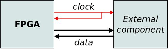
Bidirectional I/O
The main feature of source-synchronous outputs is that the related clock is generated by the FPGA. This is obviously suitable when all data signals are directed towards the external component. But even when there are data signals in both directions, it can make sense to rely on a clock that is generated by the FPGA.
However, note that the data inputs are synchronous with the clock on the PCB, and not the clock inside the FPGA chip. These two clocks have exactly the same frequency, of course. But there is a timing difference that depends on the clock-to-output delay of the output ports. This can be several nanoseconds.
It's therefore recommended to make a loopback on the PCB: Connect the FPGA's clock output to an input port. This input port can be treated as if it was a system synchronous clock: The external component behaves as if its clock came from a dedicated oscillator, and not from the FPGA. This is similar to a system synchronous clock, because both the FPGA and the external component rely on the same physical signal on the PCB.
It may also be possible to treat the data inputs as source-synchronous inputs. In particular, if the phase shifting technique is used, there is no need for a clock loopback. This is in fact the usual way to interface with DDR SDRAM memories.
The important conclusion is to plan the timing of the input signals carefully before the PCB is manufactured, and to consider adding a clock loopback if necessary.