This page is the first of three in a series about clock domains.
Introduction
Except for very trivial FPGA designs, more than one clock is used with its synchronous elements (flip-flops, block RAMs, shift registers etc). Most functional units inside a logic design are based one clock however, so most of the time, the topic of multiple clocks doesn't need any special attention. Things become more difficult when logic that is based upon one clock is connected with logic that depends on another clock. This series of pages discusses how to work with multiple clocks in a design.
When connecting logic that depends on different clocks, the first and most important question to answer is whether resynchronization logic is required. This is equivalent to asking whether the two clocks are related clocks or not. This page explains this question and how to answer it, as well as other related topics. A lot of the discussion below is related to timing constraints and the possibility to enforce them on certain elements of logic. For that reason, I shall begin with a brief recap on timing.
The discussion in this series of pages is limited to positive edge triggered flip-flops, i.e. flip-flops that react to rising edges of their clock inputs. Other synchronous elements also exist of course, i.e. logic elements that sample and produce signals based upon a clock: Shift registers, block RAMs and a whole lot of other functional elements. Some of these elements may react on the falling edge of the clock, or even on both. In the discussion here, I disregard all this for the sake of simplicity.
Also, I shall use the expression "X is synchronous with Y" to express that the synchronous element X's clock input is connected to the clock Y. Hence this synchronous element samples its input (or inputs) with this clock, and also updates its outputs with it.
Briefly on the basics of timing
This is a short summary of the theory of timing. A more detailed explanation can be found on a separate page.
Consider the following drawing, which shows the signal path from one flip-flop to another, through a LUT:
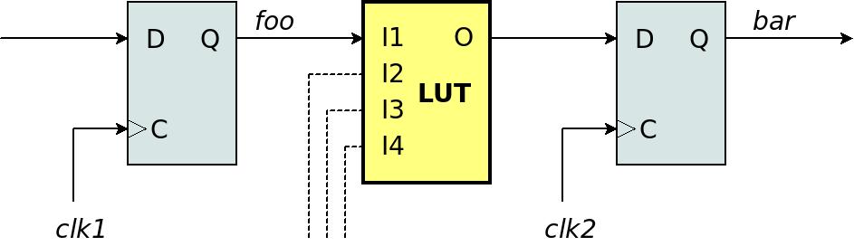
The LUT (Look-Up Table) in this drawing represents any group of combinatorial logic: Any change in I1, I2, I3 or I4 causes an immediate change in the output O, with an amount of propagation delay.
Hence the signal path goes like this: The left flip-flop's Q output, which is labeled @foo, changes after a rising edge on its input clock, @clk1. Because this output is connected to I1, the LUT's output O may change after a brief delay. This goes into the right flip-flop's data input, which is D. After a rising edge on @clk2, the flip-flop copies D into Q (which is labeled @bar).
But it's not that simple. All flip-flops have timing requirements: The data input (D) must be stable tsu (the setup time) before the @clk2's rising edge, and remain stable thold (the hold time) after this edge.
The vast majority of signal paths in an FPGA are related to a single clock, so @clk1 and @clk2 are exactly the same clock signal (we'll disregard clock skew). For such paths, it's possible to calculate whether these two timing requirements can be guaranteed.
For example, let's look at drawing above and the timing requirement for tsu: The idea is to find how much time it takes from the rising edge of @clk1 to when the D input of the flip-flop to the right is updated and stable. This is the sum of all delays on this path: It starts with the delay from the rising edge of @clk1 until @foo is updated ("clock to output"), and continues with all delays until the D input of the flip-flop to the right. This includes the delay of the LUT as well as the delays of the wiring between the logic elements (routing delays).
Because @clk1 and @clk2 are the same clock, we know when the next rising edge on both flip-flops is: It's one clock period later (e.g. 10 ns for a 100 MHz clock). So the path's total delay must be lower than the clock period, with a margin of tsu. If this can be guaranteed, it ensures what tsu requires: That the D input of the flip-flop to the right is stable with a time margin (tsu) before the rising edge of @clk2. Refer to the page about timing theory for an example with numbers.
A similar calculation can be done for thold. Unlike tsu, the requirement is that the D input of the flip-flop to the right remains stable for a certain amount of time (thold) after a rising edge of @clk2. Hence the clock period is irrelevant and is not taken into account (when @clk1 and @clk2 are the same). What matters is what happens on the same clock cycle, not the next one.
Note that calculations of this sort are possible only because we know the time difference between the rising edge of @clk1 and the rising edge of @clk2. In particular, if @clk1 and @clk2 are the same clock, this time difference that is used to calculate tsu is the clock period of that clock. But if the time difference between these two clocks is unknown, it's impossible to guarantee neither tsu nor thold.
The requirements of tsu nor thold are required by every flip-flop. This includes all flip-flops on the FPGA, of course, but also flip-flops on external devices (i.e. from an output pin of the FPGA to an external device which samples the signal with a clock). So for each flip-flop in the system, we have to ask ourselves if we have guaranteed that these two requirements are met. For flip-flops that we can't guarantee this, we have to ensure a mechanism that ensures reliable operation despite of this (i.e. resynchronization logic). This is the topic of crossing clock domains in a nutshell.
So again: When is the timing guaranteed?
Just in case you got lost in the previous section, these are the main points:
Recall that an FPGA design always includes timing constraints, which inform the design tools about on the frequencies of the clocks. Based upon this information, the tools ensure that the two timing requirements (tsu and thold) are met. Or, if the tools fail to achieve these requirements, they report this failure.
As mentioned above, it's possible to guarantee tsu and thold only when knowing the time difference between the rising edges of the clock at the beginning of the path and the clock at the end of the path. This is the case most of the time, because the larger part of a logic design consists of registers which depend on other registers that are synchronous with the same clock.
But what if two different clocks are used? If one clock is connected to the flip-flop at the beginning of the path, and another clock is connected to the flip-flop at the end of the path? In other words, what if @clk1 isn't the same as @clk2? Is it still possible to make a timing calculation and ensure the timing requirements? Well, it depends. That's what the rest of this page is about.
Clock domains and clock domain crossing
A clock domain consists of all synchronous elements (i.e. flip-flops and such) that are synchronous with a certain clock signal.
Consider this simple Verilog code snippet:
reg foo, bar;

always @(posedge clk1)
  foo <= !foo;

always @(posedge clk2)
  bar <= foo;
In this example, @foo is synchronous with @clk1, and @bar is synchronous with by @clk2. So clearly, @foo and @bar belong to different clock domains (of @clk1 and @clk2, respectively).
There's nothing to worry about @foo: It depends only on itself. However @bar is synchronous with @clk2 and depends on @foo, which is synchronous with @clk1. So can @bar be used as any register? Can we assume that @bar always obtains the value of @foo with legal timing, so its behavior is known and repeatable?
Before attempting to answer this question, let's give a name to what just happened here. It's a clock domain crossing: @foo and @bar are implemented as two flip-flops that are synchronous with different clocks. So the path from @foo to @bar goes from one clock domain to another.
More generally, clock domain crossing refers to when the output of a synchronous element that belongs to one clock domain ends up at the input of a synchronous element that belongs to another clock domain. There is often combinatorial logic between these two synchronous elements.
So even if @bar would have been defined as
always @(posedge clk2)
  bar <= !foo || !bar;
there's still a clock domain crossing here. In this case, it would have started at @foo, gone through the LUT that implements the logic function, and ended at @bar, just as shown in the drawing above.
Related clocks vs. unrelated clocks
The term related clocks refers to clocks that are derived from the same reference clock in a way that ensures predictable time differences between their rising edges and falling edges (except for known inaccuracies and jitter).
The term "synchronous clocks" is often used instead of "related clocks". Likewise, "asynchronous clocks" is commonly used instead of "unrelated clocks".
A common example of a related clock is when a single FPGA PLL is used to generate several clocks, with known relations between their frequencies. In this scenario, FPGA tools usually arrange the clock buffers so that the clock edges are aligned, to the extent possible.
For example, when a reference clock is multiplied by 2 and 3:
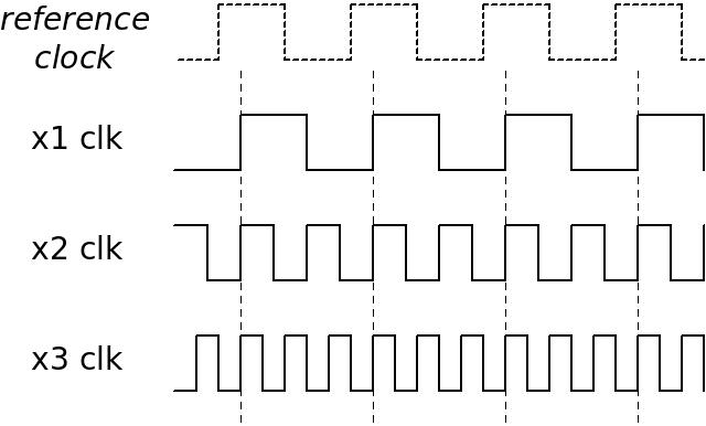
In this example, x1 clk, x2 clk and x3 clk are related clocks, as the timing between each pair of these clocks is predictable.
In the general case, the reference clock is an unrelated clock in relation to any of these other clocks: The timing between the reference clock's edges in relation to the other clocks may change with temperature and other factors. However if the PLL is configured to ensure a predictable alignment between the reference clock and the PLL's outputs, even the reference clock is a related clock.
The knowledge of time relations between clocks allows timing calculations for paths that go between their clock domains. For example, the timing of a path between the domains of the x1 clk and x2 clk is calculated with the same requirements as a path between the x2 clk and itself. This is because the shortest time difference between these two clocks is the same to the time between two rising edges of the x2 clk.
Likewise, a path between the x2 clk and x3 clk can be calculated, but the shortest time difference is just a sixth of the x1 clk's period. Therefore, the worst case timing requirement corresponds to that of an imagined x6 clk. The reason is the time difference between the second rising edge of the x2 clk and the third rising edge of the x3 clk.
See this page for a more detailed discussion on how the timing is calculated.
So the point with this example is to say something that is true even in general: With related clocks, it's possible to guarantee the timing by enforcing timing constraints on the paths between these clocks, just like paths within the same clock domain. This is possible when the FPGA tools intentionally make sure that the clock edges are aligned. As demonstrated in the example, the timing requirements are often stricter than for each of the clocks individually, and sometimes much stricter.
Note however that the fact that two clocks are derived from the same reference clock doesn't necessarily make them related clocks. In particular, if the skew between these clocks is uncontrolled or unknown (which is the case unless the design tools have explicitly used clock distribution resources with equal delays), they should be treated as unrelated clocks.
And even the clk x1 isn't necessarily related to its reference clock, even though they have exactly the same frequency. Unless these clocks are mutually aligned deliberately, their phase relation is unknown.
Because of this topic with the phase, I wrote "a certain clock signal" in the definition for a clock domain above, and not just "a certain clock". "A certain clock" could mean, for example, the same clock on the board, that is connected to two different input pins of the FPGA. "A certain clock signal", on the other hand, refers to a wire in Verilog or in the design's netlist that represents a clock signal, like @clk1 and @clk2 in the example above. It's distributed in the Verilog design by virtue of connections of ports in instantiations or with plain "assign" statements.
The fact that the clock is exactly the same signal in Verilog means that the tools will make sure to use resources that ensure a low clock skew on hardware. It also has implications on whether the tools consider the clocks as related clocks (more on this below).
Related clocks, timing constraints and resynchronization logic
Let's get back to the original question: Can @bar in the example above be used like any register? Or more generally speaking, if a flip-flop is the destination of a path that goes from one clock domain to another, can we reliably use its output just like any flip-flop's output? Which is the same as asking whether it's possible to ensure the setup time and hold time of this flip-flop, when at least one path that reaches its data input is synchronous with another clock.
The answer is simple and short: If the clocks on both sides (@clk1 and @clk2 in the example) are related clocks, then the flip-flop's output at the destination is perfectly fine, and can be used like any register, given that the proper timing constraint for this path is achieved. Otherwise, the timing at the destination can't be ensured, and resynchronization logic must be added to tackle that fact.
This page shows a complete timing analysis of a path between two related clocks.
After the lengthy discussion above, it's time to sum this up into a few simple rules:
- It's impossible to enforce timing constraints on paths between clock domains that belong to unrelated clocks.
- If there is resynchronization logic on all paths between two clock domains, there is no need to enforce timing constraints on these paths.
- If there is no resynchronization logic on a path between two clock domains, timing constraints must be enforced on this path.
The first rule is the simplest: If you can't be sure that two clocks are related clocks, make sure to have resynchronization logic on all paths between the clock domains (the next page explains how). Also make sure that no timing constraints are enforced on these paths, because that's OK according to the second rule. Unnecessary timing constraints just make things harder for the FPGA tools.
Another result of these rules is that even if the clocks are related clocks, it's OK to treat them as unrelated clocks. As just mentioned, do that by making sure to have resynchronization logic on all paths, and turning off the enforcement of timing constraints (more on this below).
And finally, if you're sure that the clocks are related clocks, there is no need for resynchronization logic, but there must be timing constraints that are correctly enforced on all paths between the clock domains.
This table summarizes this section. The table's rows are on whether there's resynchronization logic at the end of the path, and its columns are on whether the clocks are related clocks or not. The middle of the table says whether the path needs of timing constraints or not.
| The clocks are | |||
| related clocks | unrelated clocks | ||
|
Resynch- |
Not applied | Timing constraints are required on path | This is a mistake |
| applied | Timing constraints are not required on path | ||
Common mistakes
In a complex design, where signals are wired across different modules, it's easy to overlook what signal is synchronous with which clock, and hence move from one clock domain to another unknowingly.
There are two options for harmful mistakes: The first one is creating a path between clock domains of unrelated clocks without any resynchronization logic. This means that the timing is possibly violated occasionally at the destination of these paths. Like all mistakes with timing, the visible problem can be very misleading. The tools may add to the confusion if they deduce from the timing constraints that the two clocks are related clocks, and hence unnecessarily apply timing constraints to the paths. These timing constraints have no meaning on paths between unrelated clocks, but these paths will appear in the reports as if they have been handled properly. This can confuse a human reader of the timing reports into thinking that everything is fine, or maybe even that the clocks are really related clocks.
The second harmful mistake is when two clocks are related clocks and treated as such by the logic, but the tools don't consider them as such. As a result, no timing constraints are enforced on the paths between the clock domains. As a result, there's no guarantee that the timing requirements are met at the destination. Once again, this can lead to unreliable behavior. It's however possible to spot a mistake of this sort in a timing validation checkup of the design.
The only situation where a failure to notice a clock domain crossing is really harmless is between related clocks, and the FPGA tools also considers them as such (and hence enforces timing constraints to the related paths). There can still be functional bugs if the clocks have different frequencies, and the logic doesn't take this into account, but this is just like any bug in the logic.
Avoid unnecessary constraining
Quite often, a single PLL is used to create clocks with different frequencies that are intended for use by different functional units. From the designer's point of view, they are unrelated clocks, but in reality they are related clocks, and the tools usually consider them as related clocks.
Suppose for example that a PLL generates a two clocks from a reference clock with 10 MHz. One clock is 90 MHz and the second clock is 100 MHz. The intention is to use these clocks for different parts of the project, so conceptually they are unrelated clocks. But what if there is a connection between two flip-flops, so that one flip-flop is synchronous with one clock, and the second flip-flop is synchronous with the other clock?
Because the period of the first clock is 11.11 ns and the period of the second clock is 10 ns, the worst-case time difference between the rising edges is 1.11 ns (taking all possible phase combinations into account). That is equivalent to the clock period of 900 MHz. Hence the timing of the path between these two flip-flops is tight, and even if it's possible to achieve this requirement, it poses a difficulty for the tools, in particular if there are many such paths.
This isn't a theoretic case: A common pitfall is to use a dual-clock FIFO to interface between clock domains, without paying attention to whether the clocks are related clocks or not. There's no functional problem with this mistake, but since dual-clock FIFOs always have resynchronization logic, it's pointless to force the tools into enforcing timing constraints on the paths between the two clock domains. The tools may struggle to achieve these timing constraints with no purpose.
Hence it's important to pay attention to related clocks that aren't used as such, in particular clocks that come out from the same PLL: Odds are that timing constraints are enforced on paths from one clock domains to another. This enforcement has no benefit, because the resynchronization logic protects against timing violations. On the other hand, the tool's efforts to achieve the timing constraints on these paths can result in difficulties in achieving the timing constraints for the entire design.
To solve this, add timing constraints that declare the clocks as unrelated clocks. Alternatively, define false paths or maximal delays for these paths. However, in some cases this may not be necessary, so it's worth to check the timing report for these paths before doing anything about them. For example, when using a dual-clock FIFO that is provided by the FPGA tools, adequate timing constraints are often added automatically for the paths that connect between the clock domains.
Misleading timing constraints
It's important to emphasize that the FPGA tools will usually accept and enforce timing constraints between unrelated clocks. Such constraints are pointless and confusing, in particular because the related paths appear in the timing report as if their timing requirements are guaranteed. As already discussed, it's impossible to guarantee the timing of a path between clock domains that belong to unrelated clocks.
It's important to remember that the timing constraints are just a way to give the FPGA tools information about the design. If a design achieves the timing constraints, it means something only if the timing constraints are correct. So don't try to solve a clock domain crossing by just adding a timing constraint if you're not sure that the clocks are related clocks.
And once again, when it is relevant, it's a good idea to add timing constraints that define clocks as unrelated clocks, or define false paths. That doesn't only make it easier for the FPGA tools, but also avoids confusion.
Be sure the tools are informed correctly
For all reasons mentioned above, it's crucial that the FPGA design tools have the correct information on which clocks are related clocks, and which aren't. Or more precisely, that the FPGA tools apply timing constraints to all paths that are not protected by resynchronization logic (that includes paths inside clock domains, but that's irrelevant to here).
Making sure that the tools have the same perception as the logic design can be difficult however: Each FPGA design software has it's own way to make automatic assumptions on relations between clocks. The only thing that all tools appear to have in common, is that if the tool's dedicated clocking IP is used to generate two or more clocks with the same PLL, the tool will consider these clocks as related clocks. Accordingly, paths between the relevant clock domains will be timed and the timing constraints will be enforced on these paths. This enforcement is usually based upon the timing constraint that is given for the reference clock. But don't take even that for granted.
Other than that, each tool has its own way to deduce the relation between clocks, and even different tools from the same FPGA vendor may decide differently in certain situations. Most notably, Xilinx' Vivado is more inclined towards assuming that clocks are related clocks, compared to Xilinx' previous flagship tool, ISE.
So there's no general principle for all FPGA design tools, and even a specific tool can make surprising decisions. The only way to really tackle this topic is checking the timing reports, and produce timing reports for specific path groups to ensure that the timing requirements are correct where they are necessary, and nonexistent where they are unnecessary. This is a daunting task, but worth the effort.
This concludes the first page in this series. The next page goes through the basics of clock domain crossing.