This web page belongs to a group of small projects that explore the features of the Smart Zynq board.
This project is also published in HelloFPGA, which is recommended for Chinese readers.
Introduction
This tutorial explains how to connect an OV7670 camera module to the Smart Zynq and view the live video signal on the board's own HDMI output. I will also show how the raw video stream is easily saved into a file with the help of a simple Linux command.
The information in this tutorial is relevant for other types of data acquisition as well: The techniques that are shown below can be used with other sources of image data as well as other sources of digital data.
The camera module is connected to the PL (FPGA) part of the of the Zynq chip. It is hence easy to add logic that implements image processing before sending the image data to the ARM processor. As this tutorial is based upon Xillinux, the processor part of the system consists of a complete Linux distribution.
The OV7670 module was chosen for this demonstration because this hardware is cheap, popular and easy to purchase. In addition, the digital signals that this component generates are simple to understand.
However, the OV7670 has an unfortunate flaw: By default, the colors of the video stream are incorrect. This is a known problem with this camera sensor. It is possible to correct this flaw by changing a small number of registers of this camera. This tutorial is hence divided into two parts:
- How to connect the camera sensor to the Smart Zynq board, and how to read the video stream with simple Linux tools.
- How to obtain a video stream with correct colors. This part shows how Xillybus can be used to change the camera sensor's registers with the help of I2C.
Note that a large part of this tutorial explains how the implementation works. It's not necessary to understand these explanations for the purpose of using the camera.
The OV7670 module
This tutorial is based upon the camera module shown in the picture below:
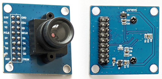
On this module, most of the pins of the pin header are connected directly to the OV7670 component. Only 3.3V and GND are connected to voltage regulators. Accordingly, all connections between the FPGA and the module are direct connections between the FPGA and the OV7670 component.
There are other modules with the same functionality on the market. It's probably OK to use these other modules as well. For example, there is a different module that has "2017/3/15" written on the PCB. This module is working properly too. On the other hand, there is a module that doesn't work properly. The module that doesn't work has "QYF-OV7670 V3.0" written on the PCB.
Another thing to be aware of is that there are different revisions of the OV7670 component. It's possible to verify that the correct revision is used on the module. How to do this is explained in the second part of this tutorial.
There are two main sources of information about the OV7670. These two documents can be found on the Internet:
- The datasheet: OV7670/OV7171 CMOS VGA (640x480) CAMERA CHIP Sensor with OmniPixel Technology, Version 1.4, August 21, 2006. It's important to obtain version 1.4 of this the document.
- The implementation guide: OV7670/OV7171 CMOS VGA (640x480) CameraChip Implementation Guide. Apparently, only Version 1.0, September 2, 2005 can be found on the Internet. This version is unfortunately outdated and refers to an earlier version of the camera chip.
Preparing the Vivado project
Create a new Vivado project from the demo bundle's zip file (the boot partition kit). Open verilog/src/xillydemo.v in a text editor. Delete the part of the code that is labeled "PART 2". Instead of that part, insert this code snippet:
   /*
    * PART 2
    * ======
    *
    * This code demonstrates a frame grabber (data acquisition) from
    * an OV7670 camera module.
    *
    */

   reg [1:0]  clkdiv;

   always @(posedge bus_clk)
     clkdiv <= clkdiv + 1;

   assign J6[10] = clkdiv[1]; // MCLK / XCLK

   assign J6[0] = 0; // PWDN, the camera is always on
   assign J6[1] = !user_w_write_32_open; // RESET#, active low

   wire [7:0] D_in;
   wire       pclk_in, hsync_in, vsync_in;

   assign D_in = J6[9:2];
   assign pclk_in = J6[11];
   assign hsync_in = J6[12];
   assign vsync_in = J6[13];

   (* IOB = "TRUE" *) reg [7:0] D_guard;
   (* IOB = "TRUE" *) reg       pclk_guard, hsync_guard, vsync_guard;

   reg [7:0]  D;
   reg 	      pclk, hsync, vsync;

   always @(posedge bus_clk)
     begin
	// Metastability guards on asynchronous inputs
	D_guard <= D_in;
	pclk_guard <= pclk_in;
	hsync_guard <= hsync_in;
	vsync_guard <= vsync_in;

	D <= D_guard;
	pclk <= pclk_guard;
	hsync <= hsync_guard;
	vsync <= vsync_guard;
     end

   wire       sample_valid;
   reg 	      previous_pclk;

   always @(posedge bus_clk)
     previous_pclk <= pclk;

   assign sample_valid = pclk && !previous_pclk;

   // wait_for_frame's purpose is to start getting data from the camera
   // at the beginning of a frame.
   reg 	      wait_for_frame;

   always @(posedge bus_clk)
     if (!user_r_read_32_open)
       wait_for_frame <= 1;
     else if (sample_valid && vsync)
       wait_for_frame <= 0;

   // fifo_has_been_full changes to '1' when the FIFO becomes full, so
   // that the data acquisition stops and an EOF is sent to the host.
   // This ensures that the data that arrives to the host is contiguous.

   reg 	      fifo_has_been_nonfull, fifo_has_been_full;
   wire       fifo_full;

   always @(posedge bus_clk)
     begin
	if (!fifo_full)
	  fifo_has_been_nonfull <= 1;
	else if (!user_r_read_32_open)
	  fifo_has_been_nonfull <= 0;

	if (fifo_full && fifo_has_been_nonfull)
	  fifo_has_been_full <= 1;
	else if (!user_r_read_32_open)
	  fifo_has_been_full <= 0;
     end

   assign user_r_read_32_eof = fifo_has_been_full && user_r_read_32_empty;

   // This part writes pixels from the camera to the FIFO

   reg 	      fifo_wr_en;
   reg [1:0]  byte_position;
   reg [31:0] dataword;

   always @(posedge bus_clk)
     if (wait_for_frame)
       begin
	  byte_position <= 0;
	  fifo_wr_en <= 0;
       end
     else if (sample_valid && hsync)
       begin
	  case (byte_position)
	    0: dataword[7:0] <= D;
	    1: dataword[15:8] <= D;
	    2: dataword[23:16] <= D;
	    3: dataword[31:24] <= D;
	  endcase

	  if (byte_position == 3)
	    fifo_wr_en <= !fifo_has_been_full;
	  else
	    fifo_wr_en <= 0;

	  byte_position <= byte_position + 1;
       end
     else
       fifo_wr_en <= 0;

   fifo_32x512 fifo_32
     (
      .clk(bus_clk),
      .srst(!user_r_read_32_open),

      .din(dataword),
      .wr_en(fifo_wr_en),
      .full(fifo_full),

      .rd_en(user_r_read_32_rden),
      .dout(user_r_read_32_data),
      .empty(user_r_read_32_empty)
      );
Alternatively, you may download xillydemo.v after this change from here.
Create a bitstream file as usual after making this change. How this Verilog code works is explained in detail below on this page.
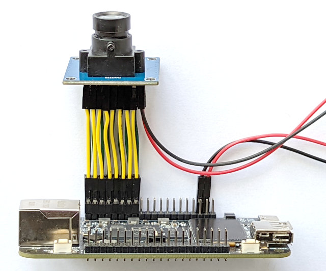
Connecting the camera module
Short Dupont jumper wires can be used to connect between the camera module and the Smart Zynq board. The length of the wires should be 10 cm or less. The optimal length is 5 cm. If the wires are longer, the quality of the digital signals may be impaired by crosstalk. Excessive noise on the horizontal sync will cause a jumping video image with green and purple stripes.
If the length of the wires is 10 cm, it may be required to change a register in order to reduce the OV7670's I/O driver current. The second part of this tutorial shows how to make this change.
This is a picture of the OV7670 module connected to a Smart Zynq SP board:
Below is a picture taken from the opposite direction. The smaller image to the top-left emphasizes that the last pin of the pin header is not connected to anything.
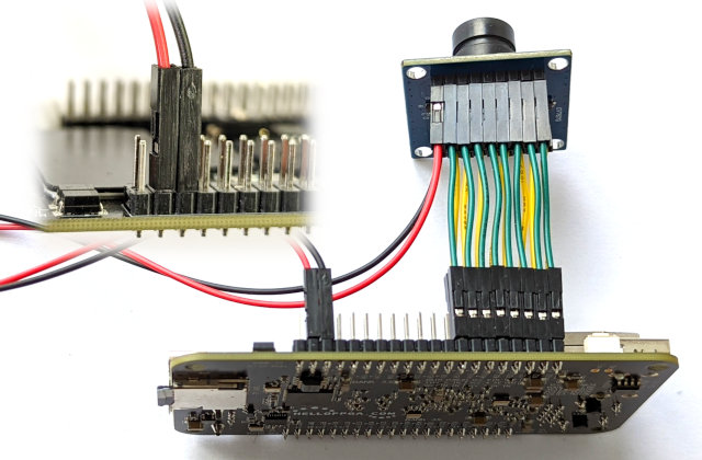
The images above show how to connect the wires: First, look for where it's written "Bank 33 VCCIO Vadj" at the back side of the Smart Zynq board. The row of pins that is close to this marking is the pin header that we shall work with. This is the pin header that is close to the HDMI connector.
There are 16 wires that are connected in parallel between the camera sensor and the Smart Zynq board. Only 3.3V and GND are connected to a different place on the pin header. These two wires don't have to be short.
Note that the pin header's last pin is 5V, so don't connect a wire to this pin.
This is the wiring specification between the camera module and the Smart Zynq's pin header. This information can be deduced from the image above as well:
| Pin header | 1 | 3 | 5 | 7 | 9 | 11 | 13 | 15 | 35 |
| Module pin | PWDN | D0 | D2 | D4 | D6 | MCLK | HS | SDA | GND |
| Module pin | RST | D1 | D3 | D5 | D7 | PCLK | VS | SCL | 3.3V |
| Pin header | 2 | 4 | 6 | 8 | 10 | 12 | 14 | 16 | 37 |
Once again, please pay extra attention to the connection of 3.3V and GND. An incorrect connection of these two wires can destroy the camera module.
Frame grabbing
Start Xillinux with a bitstream file that is based upon the updated xillydemo.v (as shown above).
This command (at shell prompt) creates a short video clip from the camera's output:
# cat /dev/xillybus_read_32 > clip.raw
This command runs for a few seconds, and then stops. This is because the data rate of the video stream is higher than the SD card's speed for writing data. This causes an overflow that stops the data flow. The mechanism behind this behavior is explained below.
It's possible to play this video clip with the following command:
# mplayer -demuxer rawvideo -rawvideo w=640:h=480:format=uyvy:size=614400:fps=31.25 clip.raw
If this command is used in a terminal window that is inside Xillinux' graphical desktop, the video is played on Xillinux' graphical interface.
It is also possible to play the video on a different computer's screen by using the technique that is described on a separate page. For example, if the other computer's IP address is 192.168.1.11, change the command so it starts with:
# DISPLAY=192.168.1.11:0 mplayer -demuxer rawvideo ...
As already mentioned, the colors of the video clip are incorrect, and the next page explains how to correct this problem.
This command reads one video frame into a file named frame.raw:
# dd if=/dev/xillybus_read_32 of=frame.raw bs=614400 iflag=fullblock count=1
The format of the raw frame is UYVY 4:2:2. In other words, each pixel consists of 16 bits. The first byte is the U component of the first pixel (or Cb). The next byte is the Y component of the same pixel. The third and forth bytes are V and Y components of the second pixel (Cr and Y).
This file can be converted into a PNG file with:
# convert -size 640x480 pal:frame.raw frame.png
There is a simple tool for viewing the image:
# display frame.png &
Live view
In order to obtain a live view of the camera, create a file named liveview.sh that contains the following:
#!/bin/bash

while [ 1 ] ; do
  dd if=/dev/xillybus_read_32 bs=614400 iflag=fullblock count=1 2>/dev/null
done | mplayer -demuxer rawvideo -rawvideo w=640:h=480:format=uyvy:size=614400 -
Run this script with
# bash liveview.sh
Why is this script needed? It's impossible to read the data from the device file directly, because mplayer is too slow. In other words, Zynq's ARM processor is not powerful enough to play the video at the correct frame rate (31.25 fps). If you try that, the video is played only briefly. The data flow stops when there is an overflow inside the FPGA.
This script is based upon an endless loop that reads a raw frame from /dev/xillybus_read_32 each time. This is the same command that was used before to read one frame into frame.raw. But this time, no output file is defined for dd. Therefore, dd writes the data to the standard output instead.
The result of this endless loop is redirected to mplayer's standard input by virtue of a pipe (pay attention to the "|" at the end of the loop). mplayer plays the video data that arrives from the standard input.
The script solves the problem with overflow because dd always reads a complete video frame. When mplayer isn't ready to accept more data, the data flow of the pipe is stopped momentarily. As a result, dd skips video frames from the camera sensor. Therefore, the frame rate that is shown on the screen is lower than the frame rate of the camera. More precisely, the frame rate that is shown is the maximal frame rate that mplayer is capable of showing.
There video image that appears on the screen is slightly delayed because of mplayer's own buffering. In order to obtain a low latency, it's necessary to write a simple program that displays the image on the screen without adding a buffer.
mplayer is a powerful media player. For example, if the incorrect colors are annoying, it's possible to play the video clip as a black and white video. Add the following part to the command in order to reduce the saturation to zero:
# mplayer -saturation -100 -demuxer rawvideo ...
End of this page's practical part
The rest of this page explains the implementation of the logic that performs the data acquisition. If you're only interested in the practical topics, continue to read on the next part of this tutorial.
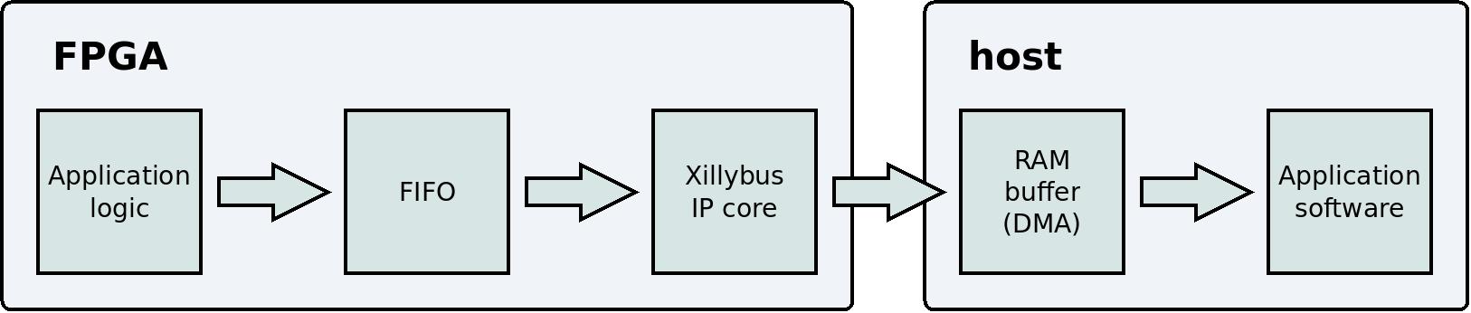
Communication between the FPGA and the host
The logic in this example is based upon the Xillybus IP core. This IP core is responsible for the communication with the host.
Recall from above that the part that was replaced in the Verilog code ends with this:
   fifo_32x512 fifo_32
     (
      .clk(bus_clk),
      .srst(!user_r_read_32_open),

      .din(dataword),
      .wr_en(fifo_wr_en),
      .full(fifo_full),

      .rd_en(user_r_read_32_rden),
      .dout(user_r_read_32_data),
      .empty(user_r_read_32_empty)
      );
This is an instantiation of a standard FIFO. This FIFO has three ports that are intended for reading data from the FIFO: rd_en, dout and empty. These ports are connected to the Xillybus IP core. This makes it possible for the IP core to read data from the FIFO and to send this data to the host. The result is that everything that is written to the FIFO reaches the device file named /dev/xillybus_read_32. In other words, a normal computer program on the host can open /dev/xillybus_read_32 as a regular file. When the program reads from this file, it receives the data that has been written to the FIFO by the application logic inside the FPGA.
The FIFO has three ports that are intended for writing data: wr_en, din and full. These ports are connected to the logic that collects the pixel data from the camera sensor. The next sections of this page explains how this logic works. For now, I just point out that the logic writes the pixel data into the FIFO with the help of @dataword and @fifo_wr_en. From this point, it's the Xillybus IP core's role to bring this data to the computer program that runs on the host. This is why this command (already mentioned above) writes this data into a file:
# cat /dev/xillybus_read_32 > clip.raw
For a general explanation about how a FIFO works, please refer to this page.
The data flow can be summarized with this diagram:
There is a section on this website about Xillybus, and this section has a page discussing data acquisition. It can be helpful to read through that page.
Note that user_r_read_32_open is connected to the FIFO's srst port. When /dev/xillybus_read_32 is opened on the host, this signal changes to high. The signal is connected with a NOT, so when the device file is closed, the FIFO is held in a reset state. This ensures that every time the file is closed, all data in the FIFO is deleted.
Interface with the camera sensor
We shall now look at the beginning of the Verilog code from above:
   reg [1:0]  clkdiv;

   always @(posedge bus_clk)
     clkdiv <= clkdiv + 1;

   assign J6[10] = clkdiv[1]; // MCLK / XCLK
@bus_clk's frequency is 100 MHz. This clock is divided by four with the help of @clkdiv. Accordingly, the camera module receives a 25 MHz reference clock. According to the camera's datasheet, this is an allowed frequency. However, the camera is designed to produce a 30 fps video stream when the reference clock's frequency is 24 MHz. The actual video frame rate is therefore slightly higher: 31.25 fps.
I should mention that this is usually an incorrect method for creating a clock. The correct method is to use a PLL or a similar resource. There is no problem with this method in this specific case, because @clkdiv is only used to create an output signal: The FPGA's own logic doesn't use this signal.
The next part in the Verilog code is this:
   assign J6[0] = 0; // PWDN, the camera is always on
   assign J6[1] = !user_w_write_32_open; // RESET#, active low
J6[0] is connected to the camera module's PWDN pin. The camera is never powered down.
J6[1] is connected to the camera's RESET#. When this pin is low, the camera is reset. @user_w_write_32_open is high when /dev/xillybus_write_32 is opened by a program on the host. So normally, the camera is not reset, because @user_w_write_32_open is low, and consequently J6[1] is high. This arrangement allows resetting the camera with the following command:
# echo 1 > /dev/xillybus_write_32
This command opens the device file for a short period of time, and this achieves the desired result.
Up to this point, I've shown how signals from the FPGA to the camera sensor are created. Now to the signals from the camera sensor to the FPGA.
The OV7670 generates a pixel clock that has the same frequency as the reference clock from the FPGA. In other words, PCLK's frequency is 25 MHz. This signal is connected to @pclk_in in the Verilog code.
The camera sensor also generates three signals that contain the video data. The names of these signals in the Verilog code are @D_in , @hsync_in and @vsync_in. The camera sensor changes the values of these signals at the same time as @pclk_in changes from high to low (falling edge). More precisely, the changes of @D_in , @hsync_in and @vsync_in are aligned with the falling edge of @pclk_in. From the FPGA's perspective, this is called a source synchronous input.
Now let's look at the relevant part in the Verilog code:
   wire [7:0] D_in;
   wire       pclk_in, hsync_in, vsync_in;

   assign D_in = J6[9:2];
   assign pclk_in = J6[11];
   assign hsync_in = J6[12];
   assign vsync_in = J6[13];

   (* IOB = "TRUE" *) reg [7:0] D_guard;
   (* IOB = "TRUE" *) reg       pclk_guard, hsync_guard, vsync_guard;

   reg [7:0]  D;
   reg 	      pclk, hsync, vsync;

   always @(posedge bus_clk)
     begin
	// Metastability guards on asynchronous inputs
	D_guard <= D_in;
	pclk_guard <= pclk_in;
	hsync_guard <= hsync_in;
	vsync_guard <= vsync_in;

	D <= D_guard;
	pclk <= pclk_guard;
	hsync <= hsync_guard;
	vsync <= vsync_guard;
     end
Note that all signals from the camera sensor are sampled with the help of @bus_clk. Even the camera's PCLK is sampled in the same way as the other signals. In other words, PCLK is not treated as a clock, but as a data signal. I'll explain this technique briefly below.
Also note that the timing relationship between @bus_clk and the camera sensor's signals is unknown. The outputs of the flip-flops that receive these signals are therefore not reliable: It's impossible to ensure the timing requirements of these flip-flops, so they can become unstable for brief time periods. This is a known problem in relation to clock domain crossing.
The solution to this problem is discussed on a separate page: Metastability guards. This means that there are two flip-flops that are connected in series to each other. The first flip-flop (@pclk_guard, for example) is connected to the external signal. The second flip-flop is connected to the first flip-flop. So even if the first flip-flop becomes unstable for a brief time, the second flip-flop's timing requirements are guaranteed. The second flip-flop's output is therefore reliable.
In conclusion: @D, @pclk, @hsync and @vsync are reliable registers (that are synchronous with @bus_clk).
Recall that @bus_clk's frequency is 100 MHz. PCLK's frequency is 25 MHz, on the other hand. So the values of @D, @hsync and @vsync should be consumed only once in every four clock cycles. But which clock cycle out of the four?
The answer is in these rows from the Verilog code:
   wire       sample_valid;
   reg 	      previous_pclk;

   always @(posedge bus_clk)
     previous_pclk <= pclk;

   assign sample_valid = pclk && !previous_pclk;
This code snippet means simply: If @pclk is high now, and it was low on the previous clock cycle, then use the values in @D, @hsync and @vsync. Recall that the camera sensor's signals change their values when the camera's PCLK changes from high to low. So when PCLK changes from low to high, the other signals are stable.
But @pclk, @D, @hsync and @vsync are registers. These registers are synchronous with @bus_clk, and they represent a snapshot of camera sensor's signals at a specific time. Instead of detecting the rising edge on PCLK itself, the logic does something similar with @pclk: When the value of @pclk changes from low to high, that's the correct time to use the values of the other registers.
This technique is called 01-signal sampling. The idea behind this technique is explained in detail on a separate page about 01-signal sampling. That page also explains how this method guarantees the FPGA's timing requirements. By doing so, the logic ensures that the values in @D, @hsync and @vsync are correct.
Starting and stopping the data flow
We shall now look at two registers which are intended to prevent transmission of data to the host:
- @wait_for_frame: The purpose of this register is to ensure that the data in the device file starts from the beginning of a frame.
- @fifo_has_been_full: This register is part of a mechanism that ensures that the data flow is halted if the FIFO becomes full.
I shall now discuss each of these two registers in detail. First, @wait_for_frame:
   reg 	      wait_for_frame;

   always @(posedge bus_clk)
     if (!user_r_read_32_open)
       wait_for_frame <= 1;
     else if (sample_valid && vsync)
       wait_for_frame <= 0;
@wait_for_frame's value is high when the device file is not opened. The value of this register changes to low in response to the camera sensor's vsync signal. This signal is high during a time period between frames. In other words, when @vsync is high, no pixel data is transmitted from the camera.
In conclusion, @wait_for_frame is high when the pixel data from the camera should be ignored: When the device file is closed, or when the device file has been opened recently but the camera is still in the middle of a frame.
I'll now move on to explaining @fifo_has_been_full: It's important to ensure that the data that arrives to the host is the same as the data that the camera sensor produces. However, an overflow may occur in the FIFO if the computer program doesn't read the data from the device file rapidly enough: The DMA buffers will eventually become full, so there will be no place to copy the content of the FIFO to. Consequently, the Xillybus IP core will not be able to read data from the FIFO. When that happens, the FIFO becomes full, making it impossible to write new data to it.
There logic can do nothing to prevent this situation. However, the logic can ensure that the data that arrives to the host is contiguous: If the FIFO becomes full, the logic stops writing data to the FIFO. In addition, when the FIFO becomes empty after the FIFO has been full, the logic requests that an EOF is sent to the host. As a result, the computer program receives all data that was written to the FIFO before the FIFO became full. After that data, the computer receives an EOF. This is the same thing that happens when the end of a regular file is reached.
This mechanism ensures that the computer program can trust that the arriving data is correct and contiguous. If the contiguity is lost, the EOF forces the computer program to close the device file. If the program opens the device file again, the data will start from a new frame, thanks to @wait_for_frame.
This is the related part in the Verilog code:
   reg 	      fifo_has_been_nonfull, fifo_has_been_full;
   wire       fifo_full;

   always @(posedge bus_clk)
     begin
	if (!fifo_full)
	  fifo_has_been_nonfull <= 1;
	else if (!user_r_read_32_open)
	  fifo_has_been_nonfull <= 0;

	if (fifo_full && fifo_has_been_nonfull)
	  fifo_has_been_full <= 1;
	else if (!user_r_read_32_open)
	  fifo_has_been_full <= 0;
     end

   assign user_r_read_32_eof = fifo_has_been_full && user_r_read_32_empty;
@fifo_has_been_full is high when the FIFO has been full. This register changes to low when the device file in not open. @fifo_has_been_full changes to high when both @fifo_full and @fifo_has_been_nonfull are high.
@fifo_full is connected to the FIFO's "full" port. But why is @fifo_has_been_nonfull necessary? The reason is that a FIFO often holds its "full" high as long as the FIFO is kept in the reset state. The purpose of this feature is to tell the application logic that the FIFO is not ready to receive data yet. The purpose of @fifo_has_been_nonfull is to prevent @fifo_has_been_full from mistakenly becoming high on this scenario.
@user_r_read_32_eof becomes high when both @fifo_has_been_full and @user_r_read_32_empty are high. In other words, an EOF is sent to the host when the FIFO has been full in the past, and is empty now. Note that in this situation, no new data will be written to the FIFO anyhow.
There is a separate page that discusses a similar solution for ensuring the contiguity of the data. The solution presented on that page is required when the two sides of the FIFO belong to different clock domains. In the code presented on this page, the FIFO is synchronous with only one clock. The implementation of @fifo_has_been_full is therefore simpler on this page.
Writing data to the FIFO
The next part in the Verilog code writes the pixel data into the FIFO:
   reg 	      fifo_wr_en;
   reg [1:0]  byte_position;
   reg [31:0] dataword;

   always @(posedge bus_clk)
     if (wait_for_frame)
       begin
	  byte_position <= 0;
	  fifo_wr_en <= 0;
       end
     else if (sample_valid && hsync)
       begin
	  case (byte_position)
	    0: dataword[7:0] <= D;
	    1: dataword[15:8] <= D;
	    2: dataword[23:16] <= D;
	    3: dataword[31:24] <= D;
	  endcase

	  if (byte_position == 3)
	    fifo_wr_en <= !fifo_has_been_full;
	  else
	    fifo_wr_en <= 0;

	  byte_position <= byte_position + 1;
       end
     else
       fifo_wr_en <= 0;
The pixel data from the camera sensor arrives as data elements that are 8 bits wide. This part of the logic reorganizes these data elements into 32 bits, so that the data can be written to the FIFO. The 8-bit Xillybus stream (/dev/xillybus_write_8) is not used for this purpose for two reasons:
- For data acquisition applications, a 32-bit stream is more suitable. The Xillybus IP core doesn't transport data as efficiently when the width of the data word is only 8/16 bits.
- /dev/xillybus_write_8 is used for I2C communication with the camera sensor, as described in the next part of this tutorial.
When @wait_for_frame is high, nothing is written to the FIFO because of one of two possibilities: The device file is not open, or the device file is open, but the beginning of a new frame has not been reached yet.
When the camera sensor's HSYNC is high, it means that the data signals contain valid pixels. The value of the expression "sample_valid && hsync" combines two criteria: When @sample_valid is high, @hsync and @D contain valid values. So if @hsync is high, the value of @D is copied into a part of @dataword. Also, if @D is copied into the last part of @dataword (i.e. @byte_position equals 3), @fifo_wr_en becomes high. As a result, @dataword is written to the FIFO. More precisely, the expression for @fifo_wr_en is like this:
fifo_wr_en <= !fifo_has_been_full;
So if @fifo_has_been_full is high, nothing is written to the FIFO, as already mentioned earlier.
The relation between Verilog code and real pins
The Verilog code above uses the inout port named J6, but how do the connections with this port reach the pin header? The answer can be found in xillydemo.xdc. This file is part of the Vivado project that creates the bitstream (in the "vivado-essentials" directory).
xillydemo.xdc contains various information that is necessary for the FPGA to work properly as an electronic component. Among others, this file contains these rows:
[ ... ]

## J6 on board (BANK33 VADJ)
set_property PACKAGE_PIN U22  [get_ports {J6[0]}];   #J6/1  = IO_B33_LN2
set_property PACKAGE_PIN T22  [get_ports {J6[1]}];   #J6/2  = IO_B33_LP2
set_property PACKAGE_PIN W22  [get_ports {J6[2]}];   #J6/3  = IO_B33_LN3
set_property PACKAGE_PIN V22  [get_ports {J6[3]}];   #J6/4  = IO_B33_LP3
set_property PACKAGE_PIN Y21  [get_ports {J6[4]}];   #J6/5  = IO_B33_LN9
set_property PACKAGE_PIN Y20  [get_ports {J6[5]}];   #J6/6  = IO_B33_LP9
set_property PACKAGE_PIN AB22 [get_ports {J6[6]}];   #J6/7  = IO_B33_LN7
set_property PACKAGE_PIN AA22 [get_ports {J6[7]}];   #J6/8  = IO_B33_LP7

[ ... ]
The first row says that the signal J6[0] should be connected to U22. This is a position on the FPGA's physical package. According to Smart Zynq's schematics, this FPGA pin is connected to the first pin of the pin header. The positions of the other ports are defined in the same manner.
Conclusion
This page showed how to obtain the pixel data from the OV7670 and send this data to the host by using the Xillybus IP core.
The next part of this tutorial explains how to use the Xillybus IP core for changing the camera sensor's registers with the help of SCCB (i.e. I2C). This is useful for changing the camera's parameters. In particular, this is necessary for obtaining an image with correct colors.