Introduction
This page explains 01-signal sampling as a method to interface with a source-synchronous input. Other strategies to interface with data sources of this sort are outlined on a page about source-synchronous inputs in general. That page also explains what a source-synchronous input is.
The idea behind 01-signal sampling is that the external clock is treated as a data signal: Accordingly, the clock is sampled by a register. This register uses an internal clock that is stable and independent of the external clock.
The data signals are sampled by additional registers. The same internal clock is used for this purpose. This internal clock is also used for all logic that implements the 01-signal sampling.
This logic detects changes on the register that is sampling the external clock. When this register changes from '0' to '1', this means that there was a rising edge on the external clock. The logic responds to this event by writing the values of the other registers to a FIFO. These registers contain the values of the data signals that were present when a rising edge of the external clock occurred.
This logic achieves the same result as if the FIFO's clock was the external clock and the FIFO's data inputs were connected directly to the data signals. The difference is which clock is used by the logic: The external clock or internal clock. The advantage of 01-signal sampling is that all logic depends only on the internal clock. This clock is stable and reliable. Even if the external clock misbehaves, the logic continues to behave in a sensible way.
The following image illustrates 01-signal sampling:
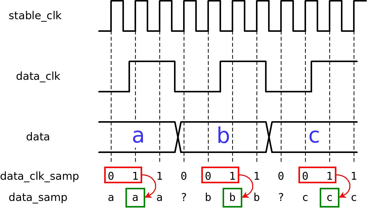
In this image, @stable_clk is the FPGA's internal clock. @data_clk and @data are signals that arrive to the FPGA. @data_clk_samp and @data_samp are registers inside the FPGA. The external signal @data_clk is represented by @data_clk_samp. The same goes for @data_samp in relation to @data.
The image illustrates that when a "0 1" pattern appears in @data_clk_samp, the value of @data_samp is written to a FIFO. This is the reason this method is called "01-signal sampling".
The FIFO is given here as an example of what to do with the arriving data. This is often a suitable solution, because the frequency of the internal clock is significantly higher than the data rate. It is therefore often convenient to continue to process the data with logic that is based upon a lower clock frequency. A FIFO is a convenient method for handing over the data to logic in a different clock domain.
It is nevertheless possible to implement the rest of the logic with the same internal clock that was used for the 01-signal sampling. Using a FIFO is only one possibility.
An example in Verilog
This Verilog code illustrates the idea. The external clock is @data_clk.
module top (
   input stable_clk,

   input data_clk,
   input [7:0] data
);

   reg [7:0] data_guard, data_samp;
   reg       data_clk_guard, data_clk_samp, data_clk_samp_d;
   wire      fifo_wr_en;

   always @(posedge stable_clk)
     begin
        data_guard <= data;
        data_clk_guard <= data_clk;

        data_samp <= data_guard;
        data_clk_samp <= data_clk_guard;

        data_clk_samp_d <= data_clk_samp;
     end

   assign fifo_wr_en = data_clk_samp && !data_clk_samp_d;

   data_fifo fifo_i
     (
      .wr_clk(stable_clk),
      .din(data_samp),
      .wr_en(fifo_wr_en),

       [ ... other ports connected here ... ]
      );
endmodule
The important part is the FIFO's wr_en: @fifo_wr_en. This signal equals "data_clk_samp && !data_clk_samp_d". Hence this signal is high as a result of detecting a "0 1" pattern on @data_clk_samp. That causes the value of @data_samp to be written into the FIFO.
Note that only @stable_clk is used as a clock by the logic. @data_clk is treated like a regular I/O input.
The timing requirements of @data_guard and @data_clk_guard are not guaranteed: The input ports are asynchronous in relation to @stable_clk. @data_guard and @data_clk_guard are hence metastability guards. The logic doesn't directly rely on the the values of these two registers. On the other hand, @data_samp and @data_clk_samp are used directly by the logic, because these registers are the second step of the metastability guard.
But does this work at all? The answer is in the timing analysis.
Timing analysis
The timing analysis of 01-signal sampling is different from the usual way: Normally, there is a constant time difference between the clock edge and moment that the data signals are sampled. This is because the clock that is used for sampling is synchronous with the data signals. But with 01-signal sampling, the sampling of @data is done with @stable_clk. Hence the moment of sampling has nothing to do with the data signals' own timing. Instead, the logic selects only the values of @data_clk_samp that are close to a rising clock edge.
So there is a random time difference between the moment of the data clock's rising edge and the moment that the actual sampling occurs. How is it possible that this method is reliable?
There is a separate page about the fundamentals of timing in a logic design. That page explains the meaning of tsu and thold. To make a long story short, a flip-flop's input port must be stable before and after the rising edge of the clock (assuming that the flip-flop is activated on a rising edge). tsu defines how much time the input port must be stable before the rising edge. thold defines how much time the input port must be stable after the rising edge. If one of these conditions is violated, the flip-flop's response to the rising edge is unpredictable.
It's possible to look at this in another way: The input port must be stable during a specific time period around the rising edge. Let's call this time period Δt = tsu + thold. Based upon Δt and other parameters, we shall now find the timing requirements that ensure reliable operation.
The entire timing analysis is based upon the situation where @data_clk_guard is high and @data_clk_samp is low. When this happens, the "0 1" pattern is detected one clock cycle later. In other words, @data_clk_samp_d will be '0' and @data_clk_samp will be '1' on the next clock cycle. @fifo_wr_en will be high as a result, so @data_samp must contain the value that the data source intended.
The analysis will therefore focus on this question: When @data_clk_guard is high and @data_clk_samp is low, what are the requirements on @data that ensure that the information arrives correctly?
The analysis will be made in two parts: In both parts, I shall assume that @data_clk_guard is high and @data_clk_samp is low. In the first part, the question will be: What is the latest moment that @data_clk can change from low to high without breaking this assumption? I shall then find the timing requirement regarding @data that ensures that @data_samp contains the correct value.
In the second part of the analysis, I will ask the opposite question: What is the earliest moment that @data_clk can change from low to high without breaking the assumption on @data_clk_guard and @data_clk_samp? I will then make a similar analysis regarding the timing requirements.
But first, let's define a few symbols:
- tclk: The clock period of @stable_clk.
- tskew: This is the skew between @data_clk and @data's ports. This is the maximal difference between the signal delays for all connections from the source of the signals to the FPGA's flip-flops.
- tj: The maximal contribution of jitter to the clock period. In other words, the time difference between two clock edges is always a value between tclk - tj and tclk + tj. Or more precisely, there is a negligible probability for a clock period that is outside these limits.
First part of the analysis
This timing diagram shows two clock cycles of @stable_clk. In the discussion below, @data_clk_guard copies its new value from @data_clk on the rising edge to the right. Likewise, @data_guard copies its new value from @data on the same clock edge.
By the same principle, @data_clk_samp and @data_samp are related to @stable_clk's rising clock edge to the left.
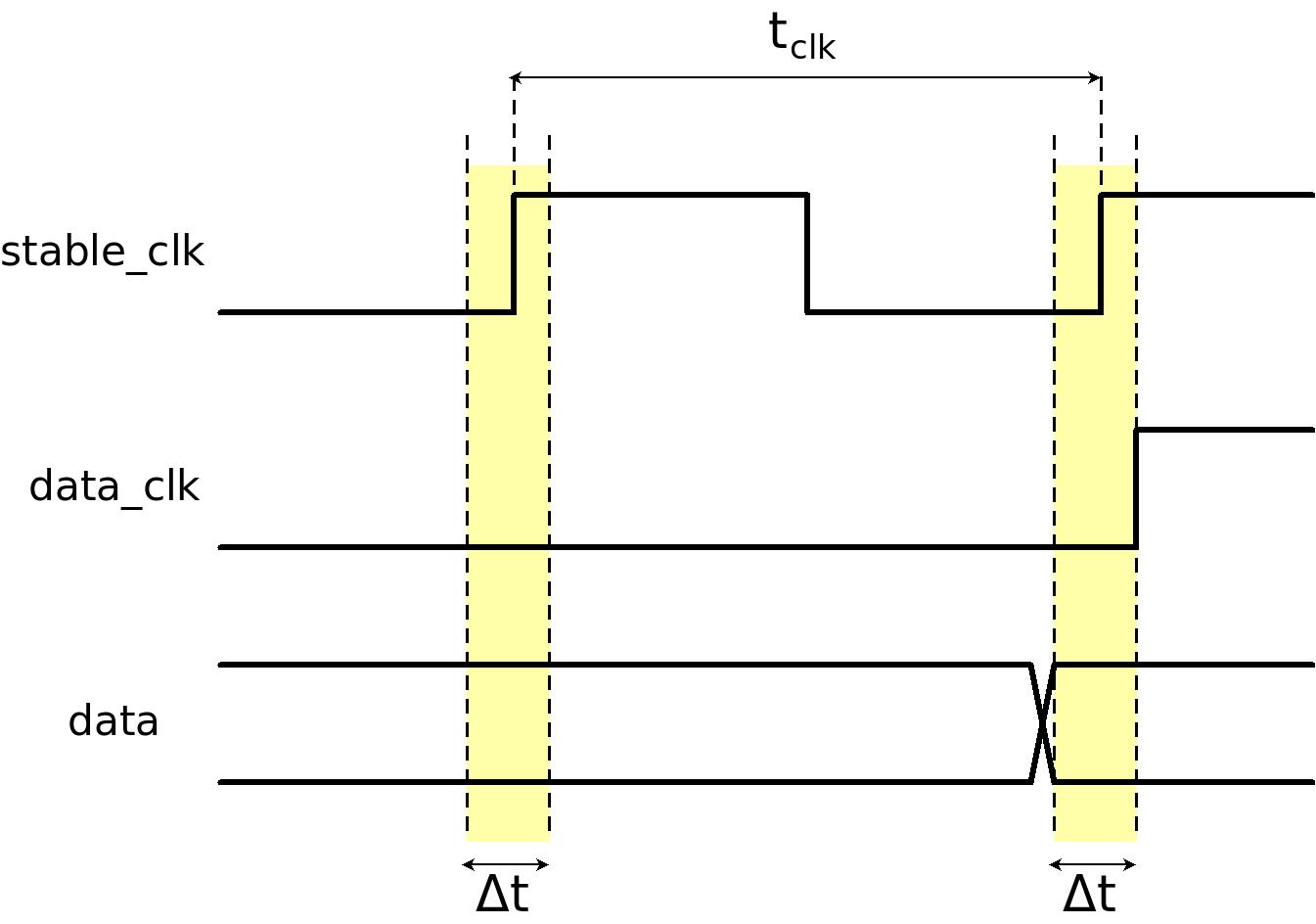
In this scenario, @data_clk changes to high exactly at the end of the yellow region. The flip-flop's timing requirements are violated, so the outcome is unpredictable. But it's possible that @data_clk_guard will be high and @data_clk_samp will be low.
However, if @data_clk changes its value a little bit later, @data_clk_guard will surely be low, because the flip-flop's behavior is predictable: In this scenario, the input port is low during the entire yellow period. This is why we can say this: If @data_clk_guard is high and @data_clk_samp is low, @data_clk changed from low to high earlier than is showed in the timing diagram above. Accordingly, the timing diagram shows the scenario where @data_clk changed at the latest possible moment.
In order to ensure that @data_guard contains a reliable value, @data must be stable before the yellow zone. This gives us the first timing requirement: @data must be stable for a time period of Δt before @data_clk's rising edge.
Note that if @data_clk changes from low to high earlier, this timing requirement still ensures the tsu requirement of @data_guard. Hence, the flip-flops' tsu is guaranteed for all scenarios where @data_clk_guard is high and @data_clk_samp is low.
The timing diagram above doesn't show anything related to skew. In order to take skew into account, the timing requirement is: @data must be stable for a time period of Δt + tskew before @data_clk's rising edge.
There is no need to take jitter into account in this scenario, because only one clock edge was involved in the discussion.
Second part of the analysis
This is the timing diagram for this scenario:
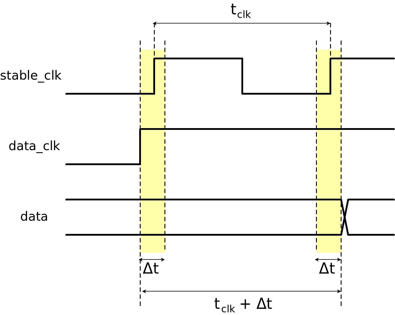
In this scenario, @data_clk changes to high exactly at the beginning of the yellow region of @stable_clk's previous clock edge.
There is no doubt that @data_clk_guard will be high in this situation. However, the value of @data_clk_samp is not predictable, because of the timing violation on the previous clock cycle. As before, it is possible that @data_clk_samp will be low. But if @data_clk changes its value earlier than this, @data_clk_samp will definitely be high.
So if @data_clk_guard is high and @data_clk_samp is low, @data_clk changed from low to high later than is showed in the timing diagram above. Accordingly, the timing diagram shows the scenario where @data_clk changed at the earliest possible moment.
In order to ensure that @data_guard contains the correct value, @data must be stable after the yellow region to the right.
According to the timing diagram above, the time difference between @data_clk's rising edge and the end of the second yellow region is Δt + tclk. But we also need to take skew and jitter into account. Therefore, @data must be stable for a time period of Δt + tclk + tskew + tj after @data_clk.
Note that if @data_clk changes from low to high earlier, this timing requirement still covers the hold requirement of @data_guard. Hence, the flip-flops' thold is guaranteed for all scenarios where @data_clk_guard is high and @data_clk_samp is low.
The timing requirements
In conclusion of the timing analysis from above, these are the two timing requirements for ensuring reliable operation of 01-signal sampling:
- @data must be stable for a time period of at least Δt + tskew before @data_clk's rising edge.
- @data must be stable for a time period of at least Δt + tclk + tskew + tj after @data_clk's rising edge.
These requirements may seem complicated, however it's often easy to ensure that they are achieved. For example, if @data changes along with the @data_clk's falling edge, it's usually easy to ensure these requirements. If @stable_clk is three times as fast as @data_clk, that is often enough.
In most cases, there is no need to know the accurate values for Δt, tskew or tj. It is often enough to calculate how large Δt and Δt + tskew + tj are allowed to be, based upon the two requirements from above. If @stable_clk's frequency is high enough, the values of these two expressions is often larger than what is realistically possible for an FPGA.
IOB registers should be used to minimize the timing differences between the FPGA's input ports (tskew). Also, timing constraints should be written in relation to these input ports for the purpose of ensuring that IOB registers are used.
Variants of 01-signal sampling
In the discussion so far, I've assumed that @data changes along with data_clk's falling edge. If @data changes along with the @data_clk's rising edge, the logic should be adjusted to instead become active when @data_clk_guard is low and @data_clk_samp is high. In other words, the logic should detect the falling edge of @data_clk by looking for a "1 0" pattern.
It's also possible to choose a different criterion for when to obtain the value of @data. For example, it may be better to delay @fifo_wr_en by a few clock cycles. Sometimes, it better if @fifo_wr_en is active earlier than suggested above. This depends on the timing relations between @data_clk and @data. Refer to the datasheet of the source of the signals, and analyze the timing as shown above.
If @data_clk's frequency is relatively high, it's possible to use DDR registers in order to sample @data_clk and @data. The logic that implements this solution is a bit more complicated, but the same principles apply.
Is @data_guard really a metastability guard?
The short answer to this question is yes. @data is asynchronous with @stable_clk, so @data_guard's timing requirements are not guaranteed.
But let's narrow down the discussion to the clock cycles where @data_guard's content is actually used: Note that the two timing requirements from above ensure that the flip-flops that implement @data_guard operate reliably. Both the tsu and the thold of these flip-flops are guaranteed.
Therefore, @data_guard isn't really used as a metastability guard. In the way that this register is used, it functions only as a delay register. But it doesn't hurt that an extra register protects against timing violations that may happen if the physical signal (@data) misbehaves. This is relevant in particular when the signal is connected to the FPGA through a connector.
A real-life example
There is an example of logic that connects with an OV7670 camera sensor on a different page. This logic obtains the pixel data from this camera sensor by virtue of 01-signal sampling. The inputs from the camera sensor are as follows:
   input       pclk_in;
   input [7:0] D_in;
   input       hsync_in, vsync_in;
The logic that performs 01-signal sampling is as follows:
   (* IOB = "TRUE" *) reg [7:0] D_guard;
   (* IOB = "TRUE" *) reg       pclk_guard, hsync_guard, vsync_guard;

   reg [7:0]  D;
   reg 	      pclk, hsync, vsync;

   wire       sample_valid;
   reg 	      previous_pclk;

   always @(posedge stable_clk)
     begin
	// Metastability guards on asynchronous inputs
	D_guard <= D_in;
	pclk_guard <= pclk_in;
	hsync_guard <= hsync_in;
	vsync_guard <= vsync_in;

	D <= D_guard;
	pclk <= pclk_guard;
	hsync <= hsync_guard;
	vsync <= vsync_guard;

        previous_pclk <= pclk;
     end

   assign sample_valid = pclk && !previous_pclk;
For the purpose of clarity, there are slight differences between the Verilog code that is presented here and the Verilog code on the page about OV7670. These differences have no impact on how the logic works.
Let's compare this Verilog code with the code that I presented at the top of this page. The names of the signals are different, but they mean the same thing: Instead of @data, we now have @D_in, @hsync_in and @vsync_in. Instead of @data_clk, we now have @pclk_in. And instead of @fifo_wr_en, we now have @sample_valid. The change in the names can be confusing, but there is no change from the Verilog code from above.
Note the "(* IOB = "TRUE" *)" parts before the declarations of the registers. When using Vivado, this is a possible way to request that the registers are inserted into the IOBs.
In this example, the FIFO isn't presented. This is because we don't want to write all data to the FIFO: When @sample_valid is high, it means that @D, @hsync and @vsync contain correct values from the camera sensor. But that doesn't mean that we want to write @D into the FIFO: It depends on @hsync and @vsync. So there is additional logic on the example for OV7670 that makes sure that only pixels are written to the FIFO.
But let's get to the interesting part: The timing analysis.
The frequency of @stable_clk in this example is 100 MHz. The frequency of @pclk_in is 25 MHz. According to OV7670's datasheet, the signals @D_in, @hsync_in and @vsync_in are guaranteed to be stable during 5 ns after @pclk_in changes from high to low (falling edge).
@pclk_in's clock cycle is 40 ns. The distance from the falling edge to the rising edge is hence 20 ns. Now let's compare with the timing requirements.
The first timing requirement was that @D_in, @hsync_in and @vsync_in must be stable for a time period of Δt before @pclk_in's rising edge. In reality, these signals are stable starting from 5 ns after the falling edge. Hence these signals are stable at least 15 ns before the next rising edge. Recall that Δt = tsu + thold. So the timing requirement is actually that tsu + thold is smaller than 15 ns. This is true for every FPGA.
The second requirement is that these signals are stable for at least a time period of Δt + tclk + tskew + tj after @pclk_in's rising edge. But these signals change only as a result of a falling edge. So the requirement is that Δt + tclk + tskew + tj is smaller than 20 ns. tclk equals 10 ns because @stable_clk's frequency is 100 MHz. The actual requirement is hence that Δt + tskew + tj is smaller than 10 ns. Once again, this is obvious with every FPGA.
This example demonstrates how the timing requirements can be ensured easily without the knowledge of the FPGA's exact timing parameters.
Conclusion
01-signal sampling is an excellent solution when the data rate is low in relation to the clock frequency that the FPGA can support: The data clock doesn't have to be stable. Also, the exact frequency of the data clock doesn't have to be known in advance. It's sufficient to guarantee the two timing requirements.
This method has additional advantages: If this clock becomes inactive for a brief moment, the only consequence is that data isn't collected during that specific time period. The damage from any malfunctions of this clock is limited to the disruption of the data flow. This will lead to a visible malfunction of the system, but this malfunction looks like a problem with the clock (and not as if the FPGA is haunted by ghosts).
So even though the sampling of the data signals has an inherent randomness, 01-signal sampling is a reliable and robust solution for a source synchronous input. The only real disadvantage is the limitation on the data rate.