This page is the first in a series of five pages about FIFOs.
Overview
The FPGA FIFO is a memory element with a simple concept: One part of the application logic writes data words on one side of the FIFO. On the other side of the FIFO, another part of application logic reads these words from it, in the same order (FIFO = First In First Out).
This data is stored inside the FIFO. The FIFO's depth is how many words of data it's capable of storing. The width (i.e. the number of bits per word) and the depth are parameters that the user configures for each FIFO.
FIFOs are probably the most commonly used IP in FPGA designs. Whenever one part of the logic generates data, and another part consumes it, the immediate solution that comes to mind is putting a FIFO between them (this is not to say that a FIFO is always the right solution, of course...).
For those who are familiar with command-line interface (in particular with UNIX / Linux), the use of FIFOs can be compared with pipes between commands: One program's output becomes the other one's input, and a magic machinery between them takes care of the rest.
Because of their ubiquitous use, there's a de-facto agreement on how an FPGA FIFO should behave. Every FPGA development software offers a way to generate a FIFO IP module for use by the application's design. Not only that, this FIFO module is very likely to have a certain set of ports that behave just like any other FPGA FIFO.
The software that is supplied by the FPGA's vendor allows creating FIFOs that fit your specific needs. It's just a matter of configuring its attributes in some GUI tool (width, depth and other attributes that I'll discuss), and the tools take care of the rest. All that is left to you is to make an instantiation of the module in your design. Unlike a lot of other tasks in the FPGA world, this task is really that simple.
As each FPGA vendor presents its own FIFO IP, it's of course important to read the documentation down to the fine print. Different FPGA vendors use slightly different terminology to describe the FIFOs. The names of the module's ports are slightly different as well. Also, each vendor offers a slightly different set of extra features and configuration options.
That said, odds are that the default settings correspond to what I'll refer to as a "baseline FIFO". On top of that, there's definitely a set of extra features that are always available.
However, the implementation of the FIFO in the logic fabric differs from one vendor to another, so understanding the meaning of the FIFO's attributes is important to make a good use of the FPGA's resources.
All in all, getting to know and understand FPGA FIFOs is a one-time effort. Once you've learned how to work with them on one FPGA, it's quite easy to do the same on another. Which is by itself a reason for their ubiquity.
The baseline FIFO
There is no written standard for FPGA FIFOs, but there's a wide agreement on how they should behave nevertheless.
All FIFOs have two interfaces, one for writing words and one for reading words. Let's look at the instantiation of what I'll call the "baseline FIFO". It has important variations, which I'll get to later.
myfifo myfifo_ins
  (
   .rst(rst),       // Asynchronous reset input

   // Write interface ports
   .wr_clk(wr_clk), // Write clock input
   .wr_en(wr_en),   // Write Enable input
   .din(din),       // Write word input
   .full(full),     // Full output

   // Read interface ports
   .rd_clk(rd_clk), // Read Clock input
   .rd_en(rd_en),   // Read Enable input
   .dout(dout),     // Read word output
   .empty(empty)    // Empty output
);
The names of the ports are those that are used by Xilinx' tools, but other FPGA vendors use similar names.
The FIFO module's ports are divided into three groups: A reset signal (@rst), which I shall get back to later. And as expected, there's a write interface and a read interface, each consisting of four ports.
Regarding @din and @dout, these are two vector ports which carry the data words that go into the FIFO and out from it. How wide these words are is something you decide when setting up the FIFO, by using the relevant software tool. You'll also set up the depth of the FIFO, i.e. how many words it can contain. These two parameters influence the amount of the FPGA's memory resources that the FIFO consumes.
Clocks
It's worth noting that each of these two interfaces has its own clock: @wr_clk and @rd_clk. The other ports in each interface are synchronous with each of these two clocks.
FIFOs are often used to move data from one clock domain to another, because they have two clocks: If some logic in your design is synchronous with clk_A, and another part is synchronous with clk_B, how do you make them work together? The first thought of any FPGA engineer is to put a FIFO between them. This is mainly because the task of crossing clock domains is a major headache, and using a FIFO solves the problem easily and safely.
The write interface
The write interface is simple: @wr_clk, @wr_en and @din are inputs to the FIFO, and @full is an output.
When @wr_en is high on the rising edge of @wr_clk, the data in @din is pushed into the FIFO. The @full port is high when the FIFO is full.
For example, this is a waveform of writing five words to the FIFO:
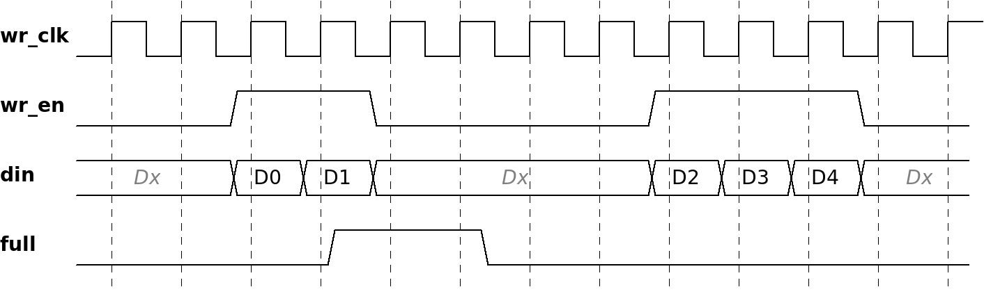
In this waveform, the application logic first writes the words D0 and D1. The FIFO raises its @full output to inform that the FIFO became full after the successful write of D1. The application logic responds to this by lowering @wr_en during the same clock cycle. After a couple of clock cycles, the FIFO changes @full to low in order to indicate that it's fine to write again. This is most likely due to activity on the other side (i.e. data has been read from the FIFO).
The application logic could have begun writing on the clock cycle for which @full changed to low, however it begins doing so slightly later (in this specific example). As shown in the waveform, three additional words are written.
In the waveform, where @din is marked with the "Dx" value, it means that the value is ignored and therefore it doesn't matter what value is there. For example, in the segment with "Dx" between D1 and D2, @din could have remained on D1, changed to D2 earlier than shown, or something completely different. The result would have been the same.
For a simple coding example, suppose I want to fill the FIFO with words that count up, whenever possible:
assign wr_en = !full;

always @(posedge wr_clk)
  if (wr_en)
    din <= din + 1;
This exemplifies the correct relation between @full and @wr_en: If @full is high, @wr_en must be low on the same clock cycle. And what if it isn't? What if we ignore the @full signal? Odds are that the FIFO will ignore the wr_en in this case. So it will probably behave as if its wr_en port was connected to @the_real_wr_en, which is defined as follows:
assign the_real_wr_en = wr_en && !full;
However some FPGA tools allow configuring the FIFO without this safety mechanism. If so, virtually anything can happen if an attempt is made to write data to the FIFO when it's full.
This way or another, @full should be respected, or else it will appear as if data has leaked away. Consider the example above: Had @wr_en been high all the time, @din would have kept on counting up, regardless of whether the data was written to the FIFO or not. So when reading the data at the other side, the counting up would have been discontinuous.
Note that @full can change from low to high only as a result of a write cycle, i.e. immediately after a rising clock edge when @wr_en is high. Except for when the FIFO is reset, as discussed further below.
The read interface
The read interface is quite similar, but not exactly the same. @rd_clk and @rd_en are inputs to the FIFO, @dout and @empty are outputs.
When @rd_en is high on the rising edge of @rd_clk, a new word is read from the FIFO's memory, and @dout is updated with its value after that rising edge, i.e. on the next clock cycle. The @empty port is high when the FIFO is empty.
In this example waveform, five words are read from FIFO:
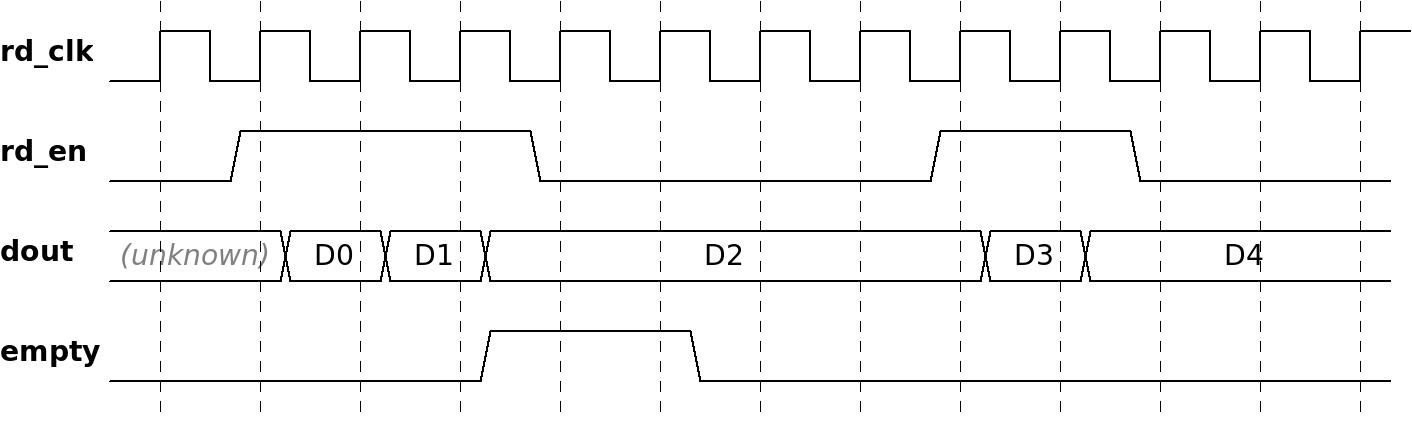
In this waveform, the application logic begins with reading three words. In response to @empty changing to high (together with D2 appearing on @dout), the application logic changes @rd_en to low in the same clock cycle. As before, it would have been fine to change @rd_en back to high again on the same clock cycle that @empty was changed to low (due to data being written into the FIFO on the other side). Instead, it waited for a few clock cycles, and then went on reading two additional words.
And now to a minor note: If you compare this waveform with the one above it, you may notice that five words were written, and five words were read. So why didn't @empty go high along with D4 appearing? Well, because I wanted to show that it's fine to stop reading even if the FIFO isn't empty. So for the sake of this imaginary example, there were additional words written to the FIFO, hence the FIFO didn't get empty after reading D4.
Note that @dout retains its value when @rd_en is low. The application logic may rely on this: @dout always contains the value of the last word that has been read from the FIFO (except for after reset).
Even more important, note that the new value of @dout appears after the rising edge when @rd_en is high. Hence the FIFO behaves like the following Verilog code:
always @(posedge rd_clk)
  if (rd_en && !empty)
    dout <= next_word_to_show;
This bogus Verilog code also demonstrates the fact that most FIFOs ignore @rd_en when @empty is high at the same clock cycle. As with the write interface, @rd_en should not be high if @empty is high on that clock cycle. Once again, sometimes the FIFO can be configured not to have this protection mechanism, so don't break this rule.
@empty can change from low to high only after a read cycle, i.e. after @rd_en is high on the rising edge of the clock. The only exception is when the FIFO is reset.
To give an example, here's a simplified Verilog code snippet (without reset) that reads words from the FIFO, and calculates the cumulative sum.
assign rd_en = want_to_read_now && !empty;

always @(posedge rd_clk)
  begin
    rd_en_d <= rd_en;

    if (rd_en_d)
      sum <= sum + dout; // Don't try this at home: @sum is never reset.
  end
For the sake of demonstration, I've added a @want_to_read_now signal, which indicates that the logic wants to read. @rd_en is nevertheless high only if the FIFO isn't empty.
Pay attention to @rd_en_d, which contains the value of @rd_en with a delay of one clock cycle. Consequently, @rd_en_d is high at the same time as when there's a new and valid value in @dout. This is why @rd_en_d is used as the condition for consuming @dout's value. The delay between @rd_en and @dout makes things a bit difficult, as demonstrated in this example.
Synchronization and latency
Because I drew the example waveforms above separately for write and read, they miss an important point: It takes a few clock cycles from writing the first word into an empty FIFO until the @empty port changes to low. Likewise, it takes a few clock cycles from reading the first word from an full FIFO until the @full port changes to low.
This happens because the information about writing into the FIFO needs to propagate across the two clock domains, before this information reaches the other side of the FIFO. The logic that is required for getting across clock domains causes a delay of a few clock cycles. Hence the @empty port responds slightly later. The same story goes with @full port.
How many clock cycles is this delay, then? It depends on a lot of things, among others the time relation between the two clocks' edges at the specific moment. In short, it's difficult to tell.
Among the things that do affect this delay is the number of synchronization stages, which is often a parameter that one can set for the FIFO. Two stages is a common choice, but a larger number can be selected. This can help to increase the FIFO's reliability, at the expense of using a bit more resources of logic. It also increases the latency of the @empty port and @full port, as just discussed.
So if you really feel like indulging your FIFO, increase the synchronization stages to three, to feel absolutely super safe.
The reset input
All FPGA FIFOs have a reset signal. Since the FIFO uses two clocks, this reset signal isn't expected to be synchronous with with any of them, so it's asynchronous. The FIFO's internal logic makes sure to synchronize the reset internally for each of the two clock domains.
So what does the reset do? Well, to begin with it, empties the FIFO and sets @empty to high. If there was any data in the FIFO, this data is lost.
As for the @full output, it's common (and recommended) that FIFOs holds this output high as a result of a reset, until the FIFO's is is ready to receive data (i.e. with write cycles). However, this behavior can be optional, so it's recommended to check this topic with the FIFO's documentation. After all, the FIFO isn't really full after a reset. Also, changing @full to high because of a reset breaks the rule that was mentioned above: @full should only change to high as a result of writing data.
It's important to be aware that it takes a few clocks cycles from the moment that the reset signal becomes active, to time when the @empty port and @full port change to high. This is because of the FIFO's synchronization logic. So things are a bit fuzzy during the few clock cycles around the activation of the reset. Make sure that the application logic doesn't attempt to neither write nor read from the FIFO during the few clock cycles around the reset.
Even though the reset signal is asynchronous, it should be the output of a register (flip-flop) of the FPGA. The reset should not be the output of combinatorial logic, as because the FIFO may receive unintended resets as a result of glitches.
In fact, many FPGA engineers incorrectly assume that connecting virtually anything to the reset port will work. The FPGA vendor might however have unexpected specifications on the reset signal. For example, this is taken from Xilinx' Product Guide for its FIFO (PG057):
If the asynchronous reset is one slowest clock wide and the assertion happens very close to the rising edge of slowest clock, then the reset detection may not happen properly causing unexpected behavior. To avoid such situations, it is always recommended to have the asynchronous reset asserted for at least 3 [ ... ] slowest clock cycles...
(Chapter 3, "Resets")
So Xilinx recommends that the reset is active for at least three clock cycles. I'm not sure how many are aware of that recommendation. By all means, read the user guide of your vendor's FIFO about how to properly generate this reset signal.
How the FIFO is implemented
Even though the vendor's software tools take care of everything to make the FIFO operate properly, it's a good idea to be aware of which resources of the FPGA are utilized, in particular for avoiding a shortage of some type of resources.
Each FPGA has its options, but I'll briefly mention a few common ones:
- Fully implemented in hardware. This usually means that a block RAM is used for storage, and on top of that, the logic that controls the FIFO is implemented in silicon rather than in the logic fabric. This doesn't save so much logic, but the implementation in silicon is probably better for high frequencies. The main drawback is that the feature set of such FIFO is limited to what is implemented in silicon, so the FIFO may be relatively limited in size, and trivial features may be missing.
- Block RAM FIFOs. This is the most common sort. The FIFO consists of the amount of block RAMs that is needed to obtain the FIFO's width and depth. The logic that controls the FIFO is implemented in logic fabric.
- Distributed RAM FIFOs. This is like Block RAM FIFOs, but logic slices are used as RAM instead of block RAMs. Recall that most FPGAs have the capability of using the slice's LUTs as RAMs, so this is an suitable option in particular when the FIFO is shallow. So this option is usually suitable when the depth is 32 words or less, but the tradeoff depends on the design and FPGA family.
- FIFOs based upon shift registers. This is the exotic version of distributed RAM FIFOs: Because slices can also behave as shift registers, it's possible to save a little logic by taking advantage of this.
This wraps up the first page in this series about FIFOs. The next page discusses common variants of FIFOs and additional features.