Introduction
This is the second post in a series of four about Partial Reconfiguration (or Dynamic Function eXchange, DFX) with Xilinx' Vivado. The intention of this post is walk through and explain the steps for enabling Partial Reconfiguration on an FPGA design. It's recommended to read the first post if you haven't done so already, as it explains the concepts behind these steps.
Xilinx has rebranded Partial Reconfiguration as "Dynamic Function eXchange" (DFX) in 2020. DFX is the expression used in Vivado's menus and informative notes. The technical term "Partial Reconfiguration" is used here nevertheless.
For simplicity, this post assumes only one reconfigurable partition in the project. Expanding this to several partitions is fairly straightforward.
The procedure described in this post starts before the project has been enabled for Partial Reconfiguration. So to break it down roughly, the steps are:
- Prepare the project for floorplanning
- Make an initial project setup for Partial Reconfiguration
- Floorplanning
- Check and correct the floorplanning by an implementation of the design
- Add a second reconfigurable module (or several modules)
- Perform implementation in order to obtain bitstream files
- Review the project
Preparation for floorplanning
More than any other task, floorplanning is the one that requires brainwork. It's a subtle balance between not wasting area of FPGA logic and making sure that both the static partition and the reconfigurable partitions won't have any considerable obstacles during place and route.
Accordingly, the majority of this post discusses this topic.
In the distant past, floorplanning was a technique that was used for timing closure. It helped the tools in placing the logic in a sensible way. As the tools for FPGA design have improved over time, it has been many years since I last saw that floorplanning helped to achieve the timing constraints. Today, the best strategy for achieving timing constraints is almost always to let the tools make the decisions.
With Partial Reconfiguration, floorplanning is a must, so the goal is not to make things worse. Doing this is usually a matter of trial and error. However, the simplest method to achieve good results is to perform an implementation of the design without floorplanning, and then start from how the logic is placed naturally. The next step is to try to organize the areas in a way that makes sense with Partial Reconfiguration, using the initial placement of the logic as a guideline.
In the plugin usage scenario, the floorplanning can be updated as the project evolves over time. This is however not the case in the Remote Update scenario, i.e. when Partial Reconfiguration is used as a means to make version updates to a design that is released: With Remote Update, all partial bitstreams must match with the initial bitstream. Accordingly, the static logic part of the design is frozen as soon as the initial bitstream is released. This means, among others, that the floorplanning must remain the same.
So even before starting with Partial Reconfiguration, the first task is to find a proper area in the FPGA for the static logic. There's no point wasting too much time on this, just get the starting point to go on with after the project is split in two pieces.
Don't get confused: The purpose of this first step is not the floorplanning itself, but to see how Vivado places the logic without restrictions, and from that decide which area should be allocated for the static logic. So these are the steps:
- Perform an implementation of the design as usual. Open the implemented design and look at the device view. Try to get an idea on how much logic resources the static design consumes, and how Vivado prefers placing them.
- It might be easier to do this if the parts that are intended as reconfigurable logic are temporarily removed from the project (but in a way that doesn't cause the static logic to be removed as well due to logic optimization).
- Make sure no logic element is selected in the Device view, do a Right-click somewhere over it, and pick "Draw Pblock". Draw a region that seems to be suitable to accommodate the static logic. Don't necessarily imitate the placement that Vivado made, but rather try finding a shape that allocates a minimal area without creating obstacles for the placement of the logic and achieving the timing constraints.
- Vivado responds with opening a dialog box saying "Create a new Pblock". It may suggest defining the Pblock by clock regions, and if so, don't do this. Request the Pblock based upon slices, DSPs and possibly other logic elements.
- With Ultrascale FPGAs, the Pblock dialog box may also suggest including IOBs. If so, unselect that option, or Vivado might get stuck later on while saving or resizing the Pblock (due to a bug in Vivado).
- Pay attention to the shape of the Pblock, in particular the range of slices. This information can be obtained from the Pblock properties pane in Vivado's GUI (under the "General" tab) or from the Tcl Console, where something like this will be written:
startgroup create_pblock pblock_1 resize_pblock pblock_1 -add {SLICE_X108Y148:SLICE_X149Y249 DSP48_X4Y60:DSP48_X5Y99 RAMB18_X4Y60:RAMB18_X6Y99 RAMB36_X4Y30:RAMB36_X6Y49} endgroup - If there are warnings in the Tcl Console, ignore them.
- When closing the implemented design, Vivado will ask if it should be saved. Choose "No", as the Pblock that was just created has no use.
Setting up a project for Partial Reconfiguration
Xilinx' UG909 suggests two work procedures for Partial Reconfiguration:
- The non-project flow (in its chapter 3), meaning that the implementation is performed by writing and running Tcl scripts explicitly.
- The project flow (in chapter 4), which corresponds to using Vivado's GUI and the scripts that are generated automatically by it.
I'll go with the project flow here, even though it has some limitations, some of which relate to the type of sources in the reconfigurable module (in particular regarding using block designs). Either way, it's better to start off with the project flow, since the scripts that it generates for implementation are a good basis for the non-project flow, if so needed.
These are the steps for turning on Partial Reconfiguration support on an existing project:
- Select Tools > Enable Dynamic Function eXchange… and click "Convert". The GUI will make sure that you know that turning the project into Partial Reconfigurable flow is irreversible, so agree with that. The Tcl command that is actually executed is
set_property PR_FLOW 1 [current_project]
- Decide on which is the top level module for the reconfigurable partition, and right-click its source file under the Project Manager's Sources pane in Vivado. Pick "Create Partition Definition…". This option is available only after enabling DFX, but you just did that.
- A "Create Partition Definition" dialog window appears, asking for two things: The name for the Partition Definition, which will be used to refer to the hierarchy in the logic. This name will refer to the place in the hierarchy, where different reconfigurable modules can be inserted. A suitable name could be "pr". The second thing, Reconfigurable Module Name, tells which logic goes into the partition. So for example, if Partial Configuration is used to replace an audio filter, sensible choices for Reconfigurable Module Name could be "lpf", "bpf", "hpf", so each name says which filter is applied. It can be the name of the top-level module, if that helps understanding what it does.
- The row of the chosen module in the Sources list will now appear with a yellow diamond shape, along with the name of the module and the instance name (say, "pr_block" and "pr_block_ins"), as defined in the Verilog / VHDL file. These names don't say anything about which logic is inserted into the partition, but rather reflect their name in the HDL. The partition and the reconfigurable module can be found in the "Partition Definitions" tab of the same Sources pane.
- If there are instantiations of IP (e.g. a FIFO) in the reconfigurable module, the IP can be added with by right-clicking its row in the main project's sources (under the "Hierarchy" pane) and select "Move to configurable module…". The equivalent in Tcl is something like:
move_files -of_objects [get_reconfig_modules lpf] [get_files /path/to/blkmem.xci]Doing this moves the IP to the "Partition Definitions" tab. - Not only this, the "Partition Definitions" tab works like a collection of source hierarchies for each reconfigurable module. For example, to add HDL files that are needed by a reconfigurable module, click "+" under this tab.
- Once the reconfigurable module is set up, define the Parent Implementation (see previous post on Parent implementations, Child implementations and the Wizard):
- Select Tools > Dynamic Function eXchange Wizard.
- Click Next on the welcome page and the page for editing reconfigurable modules.
- In the "Edit Configurations" page, click "+" to add a configuration. The default config_1 name is fine, as it doesn't matter a lot. By default, Vivado correctly selects the reconfigurable module for config_1, which is not a surprise, since it's the only one for now.
- The next screen is for adding configuration runs: Don't do this (for now).
- Finish the Wizard.
Trying perform an implementation of the project at this stage will most likely fail with an error saying something like "[DRC HDPR-30] Missing PBLOCK On Reconfigurable Cell: HD.RECONFIGURABLE cell 'pr_block_ins' must have PBLOCK assigned to itself or its descendant cells". Which means, in simple words, that floorplanning is necessary.
Floorplanning
At this stage, the project is set up just enough for the floorplanning task.
Before breaking down this task into small steps, it's worth to mention a few things to keep in mind:
- The area on the FPGA for the static logic should be made as small as possible, but without making it difficult for place and route. A rough estimation of its shape should have been obtained previously (see "Preparation for floorplanning" above).
- The shapes of both static logic and reconfigurable logic should be as simple as possible, preferably plain rectangles or other shapes that don't generate difficulties for routing.
- The static logic's routing may cross the areas of reconfigurable logic, but in the opposite is not true in most cases.
- In this floorplanning session, the shape of the reconfigurable logic is drawn. Because of the two last comments, this is the shape to keep simple.
- Be aware of the possibilities and limitations regarding floorplanning of your specific FPGA, as detailed in Chapters 6-8 in UG909. For example, if a series-7 FPGA is used, it's probably best to align the areas' limits with boundaries of clock regions.
Now breaking it down to steps:
- Start the synthesis of the project (i.e. start the synth_1 run). The synthesis of the reconfigurable module will automatically be done as an Out-of-Context run (OOC), e.g. lpf_synth_1. OOCs are explained further in the last post.
- Once the runs complete, open the synthesized design (implementation is not possible at this point, because there's no Pblock associated with the reconfigurable module).
- Draw a Pblock for the reconfigurable logic. Unlike the preparation stage, it should be associated with the reconfigurable logic, so: Make sure that the upper-left pane is open on the Netlist tab, and right-click the toplevel cell that goes into the reconfigurable partition (e.g. "pr_block_ins"). Select Floorplanning > Draw Pblock, and draw an area on the FPGA. The GUI operations to carry out are as described above (in "Preparation for floorplanning"). In other words, the selection iss based upon slices and other logic elements.
- Once again, if IOBs are suggested for inclusion in the Pblock, dont' accept this suggestion, or there's a chance Vivado will get stuck with processing it later.
- Don't work too hard on this, as there's a good chance you'll have to correct it due to Vivado's complaints about it. Once again, keep in mind that the Pblock is drawn for the reconfigurable logic, and the static logic takes the remaining area.
- Now to the Pblock Properties pane. It might be necessary to right-click the Pblock on the device view, and select Pblock Properties… for this to appear.
- Select the Properties tab (in the Pblock Properties pane).
- For series-7 FPGAs (i.e. not Ultrascale and later): In the Pblock Properties pane, it's recommended to set RESET_AFTER_RECONFIG if you want the logic to get the FPGA's internal reset after loading the partial bitstream (see the next post for more on resetting the reconfigurable module). This creates an XDC constraint like this:
set_property RESET_AFTER_RECONFIG true [get_pblocks pblock_pr_block_ins]
Among others, this constraint brings flip-flops to their default values. Note however that this has nothing to do with any resets that are defined in HDL or otherwise in the logic. Also note that on series-7 FPGAs, this feature requires that the Pblock's vertical boundaries are aligned with clock regions.
On Ultrascale FPGAs and later, this reset is always enabled. - There's also a SNAPPING_MODE property, which is undefined by default for series-7 FPGAs (which is equivalent to OFF). For some FPGAs, it will probably become necessary to set it to ROUTING or ON (which is the default for Ultrascale). I'll come to that later.
- Next, press CTRL-S to save the constraints (or click the diskette icon at the top bar). This adds a few rows to the XDC file, with something like this:
create_pblock pblock_pr_block_ins add_cells_to_pblock [get_pblocks pblock_pr_block_ins] [get_cells -quiet [list pr_block_ins]] resize_pblock [get_pblocks pblock_pr_block_ins] -add {SLICE_X40Y100:SLICE_X79Y149} resize_pblock [get_pblocks pblock_pr_block_ins] -add {DSP48_X2Y40:DSP48_X2Y59} resize_pblock [get_pblocks pblock_pr_block_ins] -add {RAMB18_X2Y40:RAMB18_X2Y59} resize_pblock [get_pblocks pblock_pr_block_ins] -add {RAMB36_X2Y20:RAMB36_X2Y29} - Close the Synthesized Design
- Reset the synth_1 run.
- Attempt to generate a bitstream (by clicking "Generate Bitstream"). The purpose of this implementation is to check if the are any flaws in the floorplanning. In other words, if Vivado issues Critical Warnings in response to such flaws. It may sound like an unprofessional way to validate the design, and yet it's easy and reliable.
Correcting the floorplanning
This is probably the least pleasant part about Partial Reconfiguration: To get the floorplanning just right. If you are doing this for the Remote Update use case, this phase is extra important, as this floorplanning will remain throughout the project's lifetime.
Corrections to the floorplanning are necessary for two main reasons: As a response to Critical Warnings, and at a later stage to optimize the usage of the FPGA: The goal is to reduce the waste of resources, and at the same time avoid creating obstacles for place and route.
Making modifications isn't difficult, as it's easy to drag a Pblock's boundaries. It's also easy to expand a Pblock with additional rectangles: Right-click the Pblock and select "Add Pblock Rectangle".
The Critical Warnings often say what corrections are necessary, and nevertheless be sure to have read the relevant chapter (6, 7 or 8) in Xilinx' user guide, UG909 regarding the limitations on floorplanning of your specific FPGA.
The rest of this section discusses possible issues with series-7 FPGA. Ultrascale FPGAs are much easier to work with.
One common error with series-7 FPGA is splitting of interconnect tile columns, for example:
[Constraints 18-993] The Pblock pblock_pr_block_ins has defined an area that causes the splitting of interconnect tile columns. Dynamic Function eXchange requires that the left and right paired interconnect tile columns cannot be split by a reconfigurable boundary.  This is caused by either the left or right edge of a Pblock boundary, or by the Pblock spanning over logic types not included in the Pblock ranges.  To avoid an unroutable situation, placement will be prohibited from both of these columns. To avoid placement restrictions, modify the Pblock to avoid splitting the two columns.
The column of the split contains interconnect tile INT_L_X48Y299  (SLICE_X79Y299 SLICE_X78Y299).
Please refer to the Xilinx document on Dynamic Function eXchange.
Resolution: Set the Pblock property SNAPPING_MODE to value of ON, or modify the column/X specification of the pblock to avoid this edge.
and
[Constraints 18-996] The split between the left and right columns occurs between a reconfigurable Pblock and Static logic. The static sites are not reconfigurable. The Pblock should be adjusted to remove the column from the Pblock, unless the excluded reconfigurable and static sites are not needed for the design. Note that adjusting the Pblock will prevent prohibits and improve placement of the design, but may reduce the routability if the removed sites were needed to span across the static logic. Failure to modify the Pblock may lead to an unplaceable design if these prohibited sites are required by the design. Resolution: Set the Pblock property SNAPPING_MODE to value of ON, or modify the column/X specification of the pblock to avoid this edge. and
To fix this, set the Pblock's SNAPPING_MODE property to ROUTING or ON (odds are that ROUTING won't be good enough, so select ON) as suggested in the first warning. Doing this will probably add a lot of constraints to the XDC file, of this sort:
set_property PROHIBIT true [get_sites SLICE_X79Y349]
set_property PROHIBIT true [get_sites SLICE_X78Y349]
[ ... ]
set_property PROHIBIT true [get_sites SLICE_X79Y191]
set_property PROHIBIT true [get_sites SLICE_X78Y191]
set_property PROHIBIT true [get_sites PMV_X0Y2]
set_property PROHIBIT true [get_sites SLICE_X36Y190]
set_property PROHIBIT true [get_sites SLICE_X37Y190]
[ ... ]
set_property PROHIBIT true [get_sites SLICE_X79Y176]
set_property PROHIBIT true [get_sites SLICE_X78Y176]
set_property PROHIBIT true [get_sites T14]
set_property PROHIBIT true [get_sites R15]
set_property PROHIBIT true [get_sites XADC_X0Y0]
set_property PROHIBIT true [get_sites SLICE_X36Y175]
set_property PROHIBIT true [get_sites SLICE_X37Y175]
[ ... ]
and it goes on.
The PROHIBIT setting for slice sites are those that silence the said Critical Warning. The other PROHIBIT assignments are added for sites of logic that are included in the geometric region, but are not allowed for Partial Reconfiguration on the FPGA that is used. Ultrascale FPGAs and later produce significantly less rows with PROHIBIT, if any at all.
For the purpose of just silencing the Critical Warning, it's probably fine to remove all rows with PROHIBIT, and leave one single row for the slices only. This is done by covering the range of slices that Vivado added in response to the change in SNAPPING_MODE. So turn this range into something like this:
set_property PROHIBIT true [get_sites -range {SLICE_X79Y0 SLICE_X79Y349}]
This is the kind of row in the XDC file that may resolve the problem with interconnect splitting without making the file huge.
Regardless, a row of this sort may also appear in the XDC file. Removing this row is apparently fine as well:
set_property HD.PLATFORM_WRAPPER true [get_cells pr_block_ins]
Reducing the XDC file to the minimum that silences Critical Warnings may appear somewhat superficial, but the alternative is a huge constraints file, which is a recipe for confusion later on. In my experience, the absence of warnings on this sort can be taken as an approval that the design's floorplan is fine.
Odds are that returning the SNAPPING_MODE property back to OFF will cause problems again, regardless of changes to the XDC.
Adding a reconfigurable module
Up till now, the implementation practically achieves the same as hierarchical design, with some extra restrictions. Even though a partial bitstream is generated, it's quite useless, since loading it retains the same design.
So the goal is to create another partial bitstream, which is based upon another configurable module. This requires adding a Child Implementation.
Be sure to have the previous post fresh in your mind before going on reading this, in particular the part on Parent Implementations and Child Implementations, as well as the Dynamic Function eXchange Wizard. Also recall from above on this post, that the "Partition Definitions" tab contains the currently defined reconfigurable modules and their sources.
Open the Dynamic Function eXchange Wizard from the Tools menu, and click Next on the welcome window.
On the Edit Reconfigurable Modules window, click "+". This opens a dialog box for adding a reconfigurable module. The only interesting thing about this dialog box is the Reconfigurable Module Name: This is the name that is used to identify the reconfigurable logic with, as already explained above.
The dialog box also requires associating this module with the name of a partition definition, but there is only one such anyhow (because this post assumes that only one partition is defined).
At least one Verilog / VHDL source file needs to be added to continue: More can be added from the "Partition Definitions" tab later on. Adding the name of the toplevel module of this reconfigurable module won't hurt, in particular if it's not clear from the source files themselves.
Back at the Wizard, click Next again, to the Edit Configurations windows. Click "+", and enter a configuration name. This name's only importance is that it appears in the Design Runs window. A name like config_2 or so is fine.
A new row appears in the list of configurations. Modify the configurable module in the column for the partition, so that each configuration has a different configurable module.
The last window is Edit Configuration Runs, for assigning runs to configurations. The easy way is to delete all runs that are listed in this window (if any) and click "automatically create configuration runs". That does what you would do manually anyhow: Create a parent run, call it "impl_1", and then create child runs, call them what you want, and make them the children of "impl_1".
The Wizard selects a configuration for each run, however that's easy to change. The only important thing is which configuration is associated with the parent run.
And by the way, if you delete all runs in the Wizard, all child runs go away, but impl_1 remains.
Finally: Implementation of the design
To generate the bitstreams, just click "Generate Bitstreams" in Vivado as usual. As already mentioned in the previous post, two or three bitstreams are created for each configuration in a Partial Reconfiguration project.
For example, on an Ultrascale FPGA the bitfiles can be:
- theproject.bit: The initial bitstream file, containing the static logic and the configurable logic that is related to current configuration.
- pr_block_ins_lpf_partial.bit: The partial bitstream that loads the reconfigurable logic that is related to current configuration.
- Only on Ultrascale, there's also pr_block_ins_lpf_partial_clear.bit: The bitstream to load before loading any partial bitstream, if the current configuration is already present in the FPGA.
Note that the same number of bitstream files is created for all implementations. In other words, the initial bitstream file is created for the Child Implementations as well, so it's perfectly possible to load the FPGA with one of the Child Implementations' initial bitstream, and continue from there.
For a simple way to load partial bitstreams over PCIe or USB 3.x, see this page.
None of the implementations should have Critical Warnings nor fail because of complaints regarding the Pblock and floorplanning in general, because such problem should have been solved already. Should a problem like this still happen, the floorplanning must be corrected as explained above.
Sometimes, when clicking "Generate Bitstream", and changes have been made only to the child implementations, Vivado might respond with "Bitstream generation has already completed and is up-to-date. Re-run anyway?". This is somewhat confusing, but clicking "Yes" will run the child implementations properly. This whole thing with Child Implementation is a bit of an add-on to Vivado, which is also why the status row during implementation says something like "write_bitstream complete. Child running".
Reviewing the results
As Partial Reconfiguration is much about placement, it's a good idea to review the implemented designs. You can open a specific implementation by right-clicking "Open Implemented Design" and then hover over the menu item saying "Open Implemented Design" (again). Then select which implementation to open from the list. If an implementation is missing in the list, it's probably already open.
Try right-clicking the top row of the reconfigurable logic in the Netlist pane of the Implemented Design view, and pick "Highlight Leaf cells". Then do the same with the static logic, with another color.
With the same right-click, there's also "Show Connectivity", which draws straight white lines between logic elements that are connected. The actual routing paths on the FPGA is of course different, so which regions of floorplanning these lines cross has no significance. Looking at connectivity can nevertheless help spotting when the overall organization of a floorplan makes the tools struggle.
It's quite normal and fine that some cells that apparently belong to the static logic are placed inside the reconfigurable area and vice versa. The thing to be wary of is if there seems to be a congestion somewhere — if the logic seems to packed too tightly in general, or in some specific region. If possible, changes in the floorplanning can help alleviate that.
Another thing to look at is the positions of partition pins. They appear as white horizontal bars in the device view, like this (click image to enlarge):
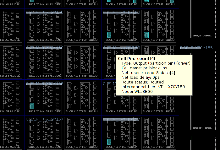
As mentioned in the previous post, partition pins can be everywhere inside the reconfigurable partition. However, if the partition pins are away from the partition's edges, it can indicate that the router struggled with timing during the Parent Implementation.
It's also possible to obtain a textual list of the partition pin's coordinates with this Tcl command (change pr_block_ins to the name of the reconfigurable logic cell):
foreach s [get_pins -of [get_cells pr_block_ins]] { set partpin [get_pplocs -quiet -pins [get_pins $s]] ; puts "$s => $partpin"; }
The coordinates for Partition pins correspond to the grid of CLBs (and not slices). On the displayed drawing, these pins are referred to as "Cell pins".
Some of the cell's pins may not be assigned a partition pin. This happens when there's a mismatch between the reconfigurable module's port list (and/or widths of vectors) and its instantiation by the static logic module. Such mismatch is perfectly legal (in Verilog), but the result may be undesired. Running this Tcl command can detect unreachable ports, in particular when this is unintentional.
This ends the technical part on setting up the Vivado project, however the next post discusses an important aspect of the FPGA design: How to ensure that the replacement of logic goes through reliably and smoothly.