介绍
这是关于 Partial Reconfiguration (或 Dynamic Function eXchange、 DFX)和 Xilinx的 Vivado的四篇系列文章中的第二篇。这篇文章的目的是介绍并解释在 FPGA 设计上启用 Partial Reconfiguration 的步骤。如果您还没有这样做,建议您阅读第一篇文章,因为它解释了这些步骤背后的概念。
Xilinx 在 2020中将 Partial Reconfiguration 重新命名为“Dynamic Function eXchange”(DFX)。 DFX 是 Vivado的菜单和信息说明中使用的表达式。尽管如此,这里还是使用了技术术语“Partial Reconfiguration”。
为简单起见,本文假设项目中只有一 reconfigurable partition 。将其扩展到几 partitions 相当简单。
在为 Partial Reconfiguration启用项目之前,本文中描述的过程就开始了。因此,粗略地分解它,步骤是:
- 为 floorplanning准备项目
- 为 Partial Reconfiguration创建一个初始 project setup
- Floorplanning
- 通过设计的实现(implementation)检查和纠正 floorplanning
- 添加第二个 reconfigurable 模块(或几个模块)
- 执行实现以获得比特流(bitstream)文件
- 审查项目
floorplanning的准备工作
floorplanning 比任何其他任务都更需要脑力劳动。这是在不浪费 FPGA 逻辑的面积和确保静态 partition (static partition)和 reconfigurable partitions 在布局和布线(place and route)期间不会有任何相当大的障碍之间的微妙平衡。
因此,这篇文章的大部分内容都讨论了这个话题。
在遥远的过去, floorplanning 是一种用于时序收敛(timing closure)的技术。它帮助工具以合理的方式放置逻辑。随着 FPGA 设计的工具随着时间的推移而改进,自从我上次看到 floorplanning 帮助实现时序约束(timing constraints)以来已经有很多年了。今天,实现时序约束的最佳策略几乎总是让工具做出决定。
有了 Partial Reconfiguration, floorplanning 是必须的,所以目标不是让事情变得更糟。这样做通常是一个反复试验的问题。但是,想要取得好的效果,最简单的方法是在没有 floorplanning的情况下,将设计的实现进行一次,然后从逻辑的自然放置方式开始。下一步是尝试以对 Partial Reconfiguration有意义的方式组织这些区域,使用逻辑的初始位置作为指导。
在 plugin 使用场景中, floorplanning 可以随着项目随着时间的推移而更新。然而,在 Remote Update 场景中情况并非如此,即当 Partial Reconfiguration 被用作对已发布的设计进行版本更新时: 对于 Remote Update,所有 partial 比特流必须与 initial 比特流匹配。因此,一旦 initial 比特流发布,设计的静态逻辑(static logic)部分就会被冻结。这意味着 floorplanning 必须保持不变。
因此,即使在开始使用 Partial Reconfiguration之前,首要任务就是在 FPGA 中为静态逻辑找到合适的区域。在这方面浪费太多时间是没有意义的,只需在项目分成两部分后开始着手。
不要混淆: 第一步的目的不是 floorplanning 本身,而是看 Vivado 如何不受限制地放置逻辑,并据此决定应该为静态逻辑分配哪个区域。所以这些是步骤:
- 照常执行设计的实现。打开 implemented 设计,看看 device view。尝试了解静态设计(static design)消耗了多少逻辑资源,以及 Vivado 更喜欢如何放置它们。
- 如果打算作为 reconfigurable 逻辑的部件暂时从项目中删除(但在某种程度上不会导致静态逻辑也因逻辑 optimization(logic optimization)而被删除),则执行此操作可能会更容易。
- 确保在 Device view中未选择逻辑单元(logic element),在其上方的某处执行 Right-click ,然后选择“Draw Pblock”。绘制一个似乎适合容纳静态逻辑的区域。不一定要模仿 Vivado 做的摆放,而是尽量找一个分配最小面积的形状,而不会给逻辑的摆放造成障碍,实现时序约束。
- Vivado 响应打开一个对话框,显示“Create a new Pblock”。它可能建议通过时钟 regions(clock regions)定义 Pblock ,如果是这样,请不要这样做。基于 slices、 DSPs 和可能的其他逻辑单元请求 Pblock 。
- 对于 Ultrascale FPGAs, Pblock 对话框可能还建议包括 IOBs。如果是这样,请取消选择该选项,否则 Vivado 可能会在稍后保存或调整 Pblock 大小时卡住(由于 Vivado中的错误)。
- 注意 Pblock的外形,尤其是 slices的范围。此信息可以从 Vivado的图形用户界面(GUI)中的 Pblock properties pane (在“General”选项卡下)或从 Tcl Console中获得,其中将写入如下内容:
startgroup create_pblock pblock_1 resize_pblock pblock_1 -add {SLICE_X108Y148:SLICE_X149Y249 DSP48_X4Y60:DSP48_X5Y99 RAMB18_X4Y60:RAMB18_X6Y99 RAMB36_X4Y30:RAMB36_X6Y49} endgroup - 如果 Tcl Console中有 warnings ,请忽略它们。
- 关闭 implemented 设计时, Vivado 会询问是否要保存。选择“No”,因为刚刚创建的 Pblock 没有用。
为 Partial Reconfiguration设置项目
Xilinx的UG909 建议 Partial Reconfiguration有两种工作流程:
- non-project flow (在其第 3 章中),这意味着实现是通过显式编写和运行 Tcl 脚本来执行的。
- project flow (第4章),对应使用 Vivado的图形用户界面和它自动生成的脚本(scripts)。
我将在这里使用 project flow ,尽管它有一些限制,其中一些与 reconfigurable 模块中 sources 的类型有关(特别是关于使用 block 设计)。无论哪种方式,最好从 project flow开始,因为如果需要,它为实现生成的脚本是 non-project flow的良好基础。
以下是在现有项目上启用 Partial Reconfiguration 支持的步骤:
- 选择 Tools > Enable Dynamic Function eXchange… 并单击“Convert”。 GUI 将确保您知道将项目变成 Partial Reconfigurable flow 是不可逆转的,所以同意这一点。实际执行的 Tcl 命令是
set_property PR_FLOW 1 [current_project]
- 确定 reconfigurable partition是哪个 top level 模块,在 Vivado的 Project Manager的 Sources pane 下右键单击它的源 file (source file)。选择“Create Partition Definition…”。此选项仅在启用 DFX后可用,但您只是这样做了。
- 出现“Create Partition Definition”对话框窗口,询问两件事: Partition Definition的名称,用于指代逻辑中的层次结构。该名称将引用层次结构中的位置,可以插入不同的 reconfigurable 模块。合适的名称可能是“pr”。第二件事, Reconfigurable Module Name,告诉逻辑进入 partition。例如,如果 Partial Configuration 用于替换 audio 滤波器,则 Reconfigurable Module Name 的合理选择可能是“lpf”、“bpf”、“hpf”,因此每个名称都说明应用了哪个过滤器。它可以是 top-level 模块的名称,如果这有助于理解它的作用。
- Sources list 中所选模块的行现在将显示为黄色菱形,以及模块和 instance name 的名称(例如,“pr_block”和“pr_block_ins”),如 Verilog / VHDL 文件中所定义。这些名称并没有说明逻辑插入到 partition中的任何内容,而是反映了它们在 HDL中的名称。 partition 和 reconfigurable 模块可以在同一 Sources pane的“Partition Definitions”选项卡中找到。
- 如果有 IP 的例化(instantiations)(例如 reconfigurable 模块中有一 FIFO) ,则可以通过在主项目的 sources 中(在“Hierarchy”窗格下)右键单击其行并选择“Move to configurable module…”来添加 IP 。 Tcl 中的等价物是就像是:
move_files -of_objects [get_reconfig_modules lpf] [get_files /path/to/blkmem.xci]这样做会将 IP 移动到“Partition Definitions”选项卡。 - 不仅如此,“Partition Definitions”选项卡的工作方式类似于每个 reconfigurable 模块的源 hierarchies (source hierarchies)集合。例如,要添加 reconfigurable 模块所需的 HDL 文件,请单击此选项卡下的“+”。
- 设置 reconfigurable 模块后,定义 Parent 实现(参见之前关于 Parent 实现、 Child 实现和 Wizard的帖子):
- 选择工具 > Dynamic Function eXchange Wizard(Tools > Dynamic Function eXchange Wizard)。
- 在欢迎页面和 reconfigurable 模块编辑页面点击 Next 。
- 在“Edit Configurations”页面,点击“+”添加一 configuration。默认的 config_1 名称很好,因为它并不重要。默认情况下, Vivado 为 config_1正确选择了 reconfigurable 模块,这并不奇怪,因为它是目前唯一的一个。
- 下一个屏幕用于添加 configuration runs: 不要这样做(暂时)。
- 完成 Wizard。
在此阶段尝试执行项目的实现很可能会失败,并出现类似“[DRC HDPR-30] Missing PBLOCK On Reconfigurable Cell: HD.RECONFIGURABLE cell 'pr_block_ins' must have PBLOCK assigned to itself or its descendant cells”的错误。这意味着,简单地说, floorplanning 是必要的。
Floorplanning
在这个阶段,项目的设置刚好可以满足 floorplanning 任务。
在将此任务分解为小步骤之前,有几点需要牢记:
- 静态逻辑在 FPGA 上的面积应该尽可能小,但不要让布局和布线变得困难。之前应该已经获得了对其形状的粗略估计(参见上面的“Preparation for floorplanning”)。
- 静态逻辑和 reconfigurable 逻辑的形状都应该尽可能简单,最好是普通的矩形或其他不会对布线(routing)产生困难的形状。
- 静态逻辑的布线可能会跨越 reconfigurable 逻辑的区域,但在大多数情况下并非如此。
- 在这 floorplanning 会话中,绘制了 reconfigurable 逻辑的形状。由于最后两条评论,这是保持简单的形状。
- 请注意有关特定 FPGA的 floorplanning 的可能性和限制,详见 UG909中的 6-8 章节。例如,如果使用 series-7 FPGA ,最好将区域的限制与时钟 regions的边界对齐。
现在将其分解为步骤:
- 启动项目的综合(synthesis)(即启动 synth_1 run)。 reconfigurable 模块的综合将自动作为 Out-of-Context run (OOC) 完成,例如 lpf_synth_1。 OOCs 将在上一篇文章中进一步解释。
- 一旦 runs 完成,打开 synthesized 设计(此时实现是不可能的,因为没有 Pblock 与 reconfigurable 模块关联)。
- 为 reconfigurable logic画一 Pblock 。与准备阶段不同,它应该与 reconfigurable 逻辑相关联,因此: 确保网表 tab(Netlist tab)上左上角的 pane 是打开的,然后右键单击进入 reconfigurable partition 的 toplevel cell (例如“pr_block_ins”)。选择 Floorplanning > Draw Pblock,在 FPGA上画一个区域。要执行的图形用户界面操作如上所述(在“Preparation for floorplanning”中)。换句话说,选择是基于 slices 和其他逻辑单元。
- 再一次,如果建议将 IOBs 包含在 Pblock中,请不要接受此建议,否则 Vivado 可能会在稍后处理它时遇到困难。
- 不要在这方面工作太努力,因为 Vivado对它的抱怨你很有可能不得不纠正它。再次记住, Pblock 是为 reconfigurable 逻辑绘制的,而静态逻辑占据剩余区域。
- 现在到 Pblock Properties pane。可能需要右键单击 device view上的 Pblock ,然后选择 Pblock Properties… 以使其显示。
- 选择属性 tab (Properties tab)(在 Pblock Properties pane中)。
- 对于 series-7 FPGAs (即不是 Ultrascale 及更高版本): 在 Pblock Properties pane中,如果您希望逻辑在加载 partial 比特流后获得 FPGA的内部复位(reset),建议设置 RESET_AFTER_RECONFIG (有关重置 reconfigurable 模块的更多信息,请参阅下一篇文章)。这将创建一个像这样的 XDC 约束:
set_property RESET_AFTER_RECONFIG true [get_pblocks pblock_pr_block_ins]
其中,此约束(constraint)将触发器(flip-flops)恢复为默认值。但是请注意,这与在 HDL 或逻辑中定义的任何复位无关。另请注意,在 series-7 FPGAs上,此功能要求 Pblock的垂直边界与时钟 regions对齐。
在 Ultrascale FPGAs 及更高版本上,始终启用此复位。 - 还有一 SNAPPING_MODE 属性,默认情况下未定义 series-7 FPGAs (相当于 OFF)。对于某些 FPGAs,可能需要将其设置为布线或 ON (这是 Ultrascale的默认值)。稍后我会谈到这一点。
- 接下来,按 CTRL-S 保存约束(或单击顶部栏中的软盘图标)。这会在 XDC 文件中添加几行,如下所示:
create_pblock pblock_pr_block_ins add_cells_to_pblock [get_pblocks pblock_pr_block_ins] [get_cells -quiet [list pr_block_ins]] resize_pblock [get_pblocks pblock_pr_block_ins] -add {SLICE_X40Y100:SLICE_X79Y149} resize_pblock [get_pblocks pblock_pr_block_ins] -add {DSP48_X2Y40:DSP48_X2Y59} resize_pblock [get_pblocks pblock_pr_block_ins] -add {RAMB18_X2Y40:RAMB18_X2Y59} resize_pblock [get_pblocks pblock_pr_block_ins] -add {RAMB36_X2Y20:RAMB36_X2Y29} - 关闭 Synthesized 设计
- 重置 synth_1 run。
- 尝试生成比特流 (通过单击“Generate 比特流”)。此实现的目的是检查 floorplanning中是否存在任何缺陷。换句话说,如果 Vivado 针对此类缺陷发布关键 Warnings (Critical Warnings)。这听起来像是一种不专业的验证设计的方法,但它既简单又可靠。
修正 floorplanning
这可能是关于 Partial Reconfiguration最不愉快的部分: 让 floorplanning 恰到好处。如果您为 Remote Update 用例执行此操作,则此阶段尤为重要,因为此 floorplanning 将在项目的整个生命周期中保留。
有两个主要原因需要对 floorplanning 进行更正: 作为对关键 Warnings的回应,以及后期优化 FPGA的使用: 目标是减少资源浪费,同时避免给布局和布线制造障碍。
进行修改并不困难,因为很容易拖动 Pblock的边界。使用其他矩形扩展 Pblock 也很容易: 右键单击 Pblock 并选择“Add Pblock Rectangle”。
关键 Warnings 经常说需要进行哪些更正,但请务必阅读 Xilinx用户指南 UG909 中有关特定 FPGA对 floorplanning 的限制的相关章节(6、7 或 8)。
本节的其余部分讨论 series-7 FPGA可能存在的问题。 Ultrascale FPGAs 更容易使用。
series-7 FPGA 的一个常见错误是拆分 interconnect tile columns,例如:
[Constraints 18-993] The Pblock pblock_pr_block_ins has defined an area that causes the splitting of interconnect tile columns. Dynamic Function eXchange requires that the left and right paired interconnect tile columns cannot be split by a reconfigurable boundary.  This is caused by either the left or right edge of a Pblock boundary, or by the Pblock spanning over logic types not included in the Pblock ranges.  To avoid an unroutable situation, placement will be prohibited from both of these columns. To avoid placement restrictions, modify the Pblock to avoid splitting the two columns.
The column of the split contains interconnect tile INT_L_X48Y299  (SLICE_X79Y299 SLICE_X78Y299).
Please refer to the Xilinx document on Dynamic Function eXchange.
Resolution: Set the Pblock property SNAPPING_MODE to value of ON, or modify the column/X specification of the pblock to avoid this edge.
和
[Constraints 18-996] The split between the left and right columns occurs between a reconfigurable Pblock and Static logic. The static sites are not reconfigurable. The Pblock should be adjusted to remove the column from the Pblock, unless the excluded reconfigurable and static sites are not needed for the design. Note that adjusting the Pblock will prevent prohibits and improve placement of the design, but may reduce the routability if the removed sites were needed to span across the static logic. Failure to modify the Pblock may lead to an unplaceable design if these prohibited sites are required by the design. Resolution: Set the Pblock property SNAPPING_MODE to value of ON, or modify the column/X specification of the pblock to avoid this edge. and
要解决此问题,请按照第一 warning中的建议将 Pblock的 SNAPPING_MODE 属性设置为布线或 ON (可能布线不够好,因此选择 ON)。这样做可能会在 XDC 文件中添加很多约束,如下所示:
set_property PROHIBIT true [get_sites SLICE_X79Y349]
set_property PROHIBIT true [get_sites SLICE_X78Y349]
[ ... ]
set_property PROHIBIT true [get_sites SLICE_X79Y191]
set_property PROHIBIT true [get_sites SLICE_X78Y191]
set_property PROHIBIT true [get_sites PMV_X0Y2]
set_property PROHIBIT true [get_sites SLICE_X36Y190]
set_property PROHIBIT true [get_sites SLICE_X37Y190]
[ ... ]
set_property PROHIBIT true [get_sites SLICE_X79Y176]
set_property PROHIBIT true [get_sites SLICE_X78Y176]
set_property PROHIBIT true [get_sites T14]
set_property PROHIBIT true [get_sites R15]
set_property PROHIBIT true [get_sites XADC_X0Y0]
set_property PROHIBIT true [get_sites SLICE_X36Y175]
set_property PROHIBIT true [get_sites SLICE_X37Y175]
[ ... ]
它继续。
slice 站点的 PROHIBIT 设置是那些使上述关键 Warning(Critical Warning)静音的设置。为几何区域中包含的逻辑的站点添加了其他 PROHIBIT 分配,但在所使用的 FPGA 上不允许用于 Partial Reconfiguration 。 Ultrascale FPGAs 和更高版本使用 PROHIBIT生成的行数明显减少(如果有的话)。
出于使关键 Warning静音的目的,使用 PROHIBIT删除所有行可能没问题,只为 slices 保留一行。这是通过覆盖 Vivado 为响应 SNAPPING_MODE的变化而添加的 slices 范围来完成的。所以把这个范围变成这样的东西:
set_property PROHIBIT true [get_sites -range {SLICE_X79Y0 SLICE_X79Y349}]
这是 XDC 文件中的这种行,可以解决 interconnect splitting 的问题,而不会使文件变大。
无论如何,这种行也可能出现在 XDC 文件中。删除这一行显然也很好:
set_property HD.PLATFORM_WRAPPER true [get_cells pr_block_ins]
将 XDC 文件减少到使关键 Warnings 静音的最小值可能看起来有些肤浅,但替代方案是一个巨大的约束文件,这会在以后造成混乱。根据我的经验, warnings 没有出现在这种情况下可以被视为设计的 floorplan 很好。
很可能将 SNAPPING_MODE 属性返回给 OFF 会再次导致问题,无论对 XDC的更改如何。
添加 reconfigurable 模块
到目前为止,实现几乎达到了与 hierarchical 设计相同的效果,但有一些额外的限制。即使生成了 partial 比特流,它也没什么用,因为加载它会保留相同的设计。
所以目标是创建另一个 partial 比特流,它基于另一个 configurable 模块。这需要添加 Child 实现。
在继续阅读本文之前,一定要记得之前的文章,特别是关于 Parent 实现和 Child 实现以及 Dynamic Function eXchange Wizard的部分。还记得在这篇文章的上面,“Partition Definitions”选项卡包含当前定义的 reconfigurable 模块和它们的 sources。
从工具菜单中打开 Dynamic Function eXchange Wizard ,然后在欢迎窗口中单击 Next 。
在 Edit Reconfigurable 模块窗口中,单击“+”。这将打开一 dialog box 以添加 reconfigurable 模块。这 dialog box 唯一有趣的是 Reconfigurable Module Name: 如上所述,这是用于标识 reconfigurable 逻辑的名称。
该对话框还要求将此模块与 partition definition的名称相关联,但无论如何只有一个(因为本文假设只定义了一 partition )。
至少需要添加一 Verilog / VHDL source file 才能继续: 稍后可以从“Partition Definitions”选项卡中添加更多内容。添加这个 reconfigurable 模块的 toplevel 模块的名称不会有什么坏处,特别是如果从源(source)文件本身不清楚的话。
返回 Wizard,再次单击 Next ,进入 Edit Configurations 窗口。点击“+”,输入 configuration 名称。此名称唯一重要的是它出现在设计 Runs (Design Runs)窗口中。像 config_2 这样的名字就可以了。
configurations列表中出现一个新行。修改 partition一栏中的 configurable 模块,使每 configuration 都有不同的 configurable 模块。
最后一个窗口是 Edit Configuration Runs,用于将 runs 分配给 configurations。简单的方法是删除此窗口中列出的所有 runs (如果有),然后单击“automatically create configuration runs”。无论如何,这可以完成您手动执行的操作: 创建一 parent run,叫它“impl_1”,然后再创建 child runs,随便叫什么,把它们变成“impl_1”的 children 。
Wizard 为每 run选择一 configuration ,但是这很容易更改。唯一重要的是哪 configuration 与 parent run相关联。
顺便说一句,如果你删除 Wizard中的所有 runs ,所有 child runs 都消失了,但 impl_1 仍然存在。
最后: 设计的实现
要生成比特流,只需像往常一样在 Vivado 中单击“Generate 比特流”即可。正如在上一篇文章中已经提到的,在 Partial Reconfiguration 项目中为每 configuration 创建了两个或三个比特流(bitstreams)。
例如,在 Ultrascale FPGA 上, bitfiles 可以是:
- theproject.bit: initial 比特流文件,包含静态逻辑和与当前 configuration相关的 configurable 逻辑。
- pr_block_ins_lpf_partial.bit: partial 比特流加载与当前 configuration相关的 reconfigurable 逻辑。
- 仅在 Ultrascale上,还有 pr_block_ins_lpf_partial_clear.bit: 如果当前 configuration 已经存在于 FPGA中,则在加载任何 partial 比特流之前加载比特流。
请注意,为所有实现创建相同数量的比特流文件。换句话说, initial 比特流文件也是为 Child 实现创建的,因此完全可以使用 Child 实现的 initial 比特流之一加载 FPGA ,然后从那里继续。
有关通过 PCIe 或 USB 3.x加载 partial 比特流的简单方法,请参阅此页面。
实现不应该有关键 Warnings 也不会因为对 Pblock 和 floorplanning 的投诉而失败,因为这样的问题应该已经解决了。如果这样的问题仍然发生, floorplanning 必须按照上述说明进行纠正。
有时,当单击“Generate 比特流”时,仅对 child 实现进行了更改, Vivado 可能会响应“比特流 generation has already completed and is up-to-date. Re-run anyway?(Bitstream generation has already completed and is up-to-date. Re-run anyway?)”。这有点令人困惑,但单击“Yes”将正确运行 child 实现。 Child 实现的整个过程有点像 Vivado的附加组件,这也是为什么实现期间的 status 行会显示类似“write_bitstream complete. Child running”的原因。
审查结果
由于 Partial Reconfiguration 非常注重放置,因此查看 implemented 设计是一个好主意。您可以通过右键单击“Open Implemented 设计”打开特定的实现,然后将鼠标悬停在显示“Open Implemented 设计”的菜单项上(再次)。然后从列表中选择要打开的实现。如果列表中缺少实现,它可能已经打开。
尝试在 Implemented 设计视图的网表 pane (Netlist pane)中右键单击 reconfigurable 逻辑的顶行,然后选择“Highlight Leaf cells”。然后用另一种颜色对静态逻辑做同样的事情。
同样的右击,还有“Show Connectivity”,在相连的逻辑单元之间画出白直线。 FPGA 上的实际布线路径(routing paths)当然是不同的,所以这些线交叉在 floorplanning 的哪些区域没有意义。然而,查看连接性有助于发现 floorplan 的整体组织何时使工具变得困难。
一些显然属于静态逻辑的 cells 被放置在 reconfigurable area 内部,反之亦然,这是很正常的。需要注意的是,如果某处似乎出现拥堵——如果逻辑总体上或在某些特定区域似乎过于紧凑。如果可能的话, floorplanning 的变化可以帮助缓解这种情况。
另一个要看的是 partition 引脚的位置。它们在 device view中显示为白色水平条,如下所示(点击图片放大):
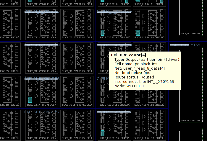
如前文所述, partition 引脚可以在 reconfigurable partition内部随处可见。但是,如果 partition 引脚远离 partition的边缘,则可能表明 router 在 Parent 实现期间与时序(timing)发生了冲突。
也可以使用此 Tcl 命令获取 partition 引脚坐标的文本列表(将 pr_block_ins 更改为 reconfigurable logic cell的名称):
foreach s [get_pins -of [get_cells pr_block_ins]] { set partpin [get_pplocs -quiet -pins [get_pins $s]] ; puts "$s => $partpin"; }
Partition 引脚的坐标对应于 CLBs 的网格(而不是 slices)。在显示的图纸上,这些引脚称为“Cell 引脚”。
某些 cell的引脚可能未分配 partition 引脚。当 reconfigurable 模块的端口 list (port list)(和/或 vectors的宽度)与静态逻辑模块(static logic module)的例化之间不匹配时,就会发生这种情况。这种不匹配是完全合法的(在 Verilog中),但结果可能是不希望的。运行此 Tcl 命令可以检测到无法访问的端口,尤其是在无意的情况下。
关于设置 Vivado 项目的技术部分到此结束,但是下一篇文章将讨论 FPGA 设计的一个重要方面:如何确保逻辑的更换可靠且顺利进行。