This is the first post in a series of four about Partial Reconfiguration, or Dynamic Function eXchange (DFX) with Xilinx' Vivado. The intention of this post is to explain the main concepts of this topic. This prepares the ground for the next post, which outlines the practical steps for setting up an FPGA project with Partial Reconfiguration.
Introduction
Partial reconfiguration is a technique that allows replacing the logic of some parts of the FPGA, while its other parts are working normally. This consists of feeding the FPGA with a bitstream, exactly like the initial bitstream that programs its functionality on powerup. However the bitstream for Partial Reconfiguration doesn't cause the FPGA to halt. Instead, it works on specific logic elements, and updates the memory cells that control their behavior. It's a hot replacement of specific logic blocks.
Xilinx' FPGAs support this feature since Virtex-4 (and Intel's FPGAs starting from Series-V).
This post walks through the concepts behind Partial Reconfiguration without getting into the hands-on technical details, as a preparation for the next post, which does exactly that. Because everything is related to everything in this topic, it's important to understand the whole framework before breaking it down to individual actions.
Explain that again?
Let's start with how the functionality of an FPGA is changed without Partial Reconfiguration. Let's say that there's an instantiation of a module somewhere in the design hierarchy. For example, in Verilog:
   moduleA reconfig_ins
     (
      .clk(clk),
      .this(this_w),
      .that(that_w),
 [ ... ]
      );
or in VHDL:
  reconfig_ins : moduleA
    port map(
      clk        => clk,
      this       => this_w,
      that       => that_w,
 [ ... ]
      );
Obviously, there's a module that is called moduleA.v or moduleA.vhd somewhere in the project, or an IP called moduleA, that populates the instantiation (along with its submodules). So we perform an implementation of the project and obtain a bitstream file, and load the FPGA with it. So far, the usual procedure.
But now, let's say that we write moduleB instead of moduleA in the code above, and perform an implementation of the logic to obtain a bitstream file. For this to work, there must be a moduleB.v or moduleB.vhd, or an IP called moduleB in the design.
We now have two bitstream files, that differ in the logic that is inside the instance that is called reconfig_ins . To switch between these two bitstreams, we need to load the entire FPGA with the desired bitstream. This involves an interruption of the FPGA's operation.
Partial Reconfiguration is a technique that allows changing from one version to another without this interruption: The FPGA keeps working normally, while the logic in reconfig_ins changes from moduleA to moduleB, and vice versa. Almost needless to say, this isn't possible just by an implementation of the two designs separately.
moduleA and moduleB are referred to as Reconfigurable Modules (RM), which means that their logic can be injected into the FPGA by virtue of Partial Reconfiguration.
Motivation
There are several reasons for using Partial Reconfiguration, such as:
- To allow Remote Update of the FPGA's logic without writing to flash memory. For example, if the FPGA is connected to a computer through PCIe, it's often desirable to upgrade the FPGA's logic along with a upgrade of the host's software. To ensure that both sides' versions are in sync, it's natural to store the FPGA's bitstream on the computer, and load the FPGA using the PCIe interface (see this page for an easy way to achieve this).
- For large FPGAs, the time it takes to load the bitstream can be too long if it includes all logic. This can be solved by using compressed bitstreams, and implement the minimal necessary logic in the initial bitstream. This way, the FPGA begins working quickly, in order to fulfill the absolutely necessary needs. The rest of the logic is loaded in a second stage, performing Partial Reconfiguration. This is often referred to as Tandem Configuration.
- To reduce FPGA cost by reusing logic resources for different tasks, that aren't necessary to work simultaneously. For example, if the FPGA implements one of several image filters, only the image filter that is currently in use occupies FPGA logic. When a different filter is needed, the region in the FPGA that is allocated for the filter is reloaded, while the rest of the FPGA keeps running normally.
- To update specific logic elements through JTAG, e.g. block RAMs that contain the executable code of a microprocessor that runs on the FPGA. This allows quick development cycles of the software.
- To insert a data probe and/or debugging tool to a design that is running on the FPGA. Partial Reconfiguration useful in particular for problems that come and go from one design implementation to another of the FPGA (which indicates a fundamental flaw in the design regarding clocking, timing etc., but that's a different story).
The partial bitstream
If you have some experience with FPGA design, odds are that you're used to a simple routine: Make some edits to the design's source code (and IPs), kick off the implementation tools, and check that it went through OK. Then load the bitstream into the FPGA through JTAG. Or alternatively, load a flash device with an image of the bitstream.
Because this is what we're all used to, it's easy to mistake the bitstream for just being a lot of data that fills the entire FPGA with mystical information on how each logic element should behave. In reality, a bitstream consists of a series of commands that are executed sequentially by the FPGA as it's loaded. Indeed, the common bitstream loads the entire FPGA with information, but it's done with several commands that control the procedure's progress. A more important aspect of these commands is that they determine which logic elements are loaded with each piece of data.
Since the bitstream itself says which logic elements are affected, it's possible to make a bitstream that alters only some logic elements, and leaves other logic elements intact. That's the cornerstone for Partial Reconfiguration.
Having said that, the partial bitstream must be compatible with the logic that is already loaded in the FPGA. It's not just a matter of overwriting the wrong logic elements: The initial bitstream is tightly coupled with the partial bitstream, in particular because the initial bitstream uses logic and routing resources that are inside the area that is changed by the partial bitstream. When the partial bitstream is set up correctly with respect to the initial bitstream, this delicate dance goes by unnoticed. If not, the FPGA will most likely go crazy, including the functionality that should have remained untouched.
Loading the partial bitstream
The delivery of a Partial Configuration bitstream to the FPGA can be done with any interface that allows loading bitstreams, as long as the process can be done while the FPGA is running. This includes the JTAG interface, so a .bit file for Partial Configuration can be loaded with the Hardware Manager as usual. But even more interesting, it can be done from inside the FPGA's own logic, by using the dedicated Internal Configuration Access Port (ICAP). This port can be used only for Partial Reconfiguration, since the part in the FPGA's logic fabric that loads the bitstream must remain intact throughout the process.
The ICAP is just an interface to the FPGA's subsystem for loading bitstreams, and doesn't dictate anything about the source of the bitstream. Accordingly, there is no limitation on how the bitstream data reaches the FPGA, or where and how it's stored. It just has to somehow be available to the piece of FPGA logic that feeds the ICAP.
For example, Xillybus offers a simple means for sending a bitstream file to the ICAP from a computer over a PCIe or USB 3.x interface, if the board has such.
Static logic
To get Partial Reconfiguration done correctly, one must give respect to the opposite part: The static logic. It's a general term for the parts in the FPGA design that must remain untouched, and are hence present from when the initial bitstream was loaded.
This logic is static in two aspects: The functional aspect, which means that the logic consists of the parts in the FPGA design (HDL and IP) that will function without interruption from the FPGA's initial start. The second aspect, which is no less important, is that the placement of this logic is limited to sites in the logic fabric that are allocated as static. On these sites, any later manipulations are not allowed.
In a real-life design, it's not enough that the static logic remains unchanged, but it's also important it continues to function properly while other parts of the FPGA are changed. As there are almost certainly nets that connect between the static logic and the the logic that changes, it's the FPGA designer's responsibility to make sure everything runs smoothly. The third post in this series discusses this.
Separation of static logic and reconfigurable logic
For Partial Reconfiguration to be even possible, there must be a strict separation between the static logic and reconfigurable logic. In particular, the physical logic elements on the FPGA must be separated, so that none of the sites that contain static logic are affected as the FPGA is loaded with the bitstream.
To understand what this requires, let's first look at what we are all used to.
Recall that the regular FPGA implementation process starts with a synthesis of the HDL design. Note that instantiation of modules in HDL doesn't imply any separation between them. The opposite is true: The synthesizer treats instantiations as a description of how the logic should work. Accordingly, the synthesizer is free to consider the entire design as one big, flat, piece of logic. Optimizations that cross the boundaries of modules are not only allowed, but are desired and occur a lot. For example, if a register in module X happens to be equivalent to some completely unrelated register in module Y, one of the registers is removed, and the remaining one is used in both modules (unless the synthesizer is specifically told to refrain from that).
Once the synthesis of the HDL is complete, the synthesized netlist is mixed with those of the design's IPs (if any).
Next, this big chunk of logic elements is placed all over the FPGA's logic fabric, and wires are routed in the way that achieves the timing constraints and other goals. Logic that belongs to different parts of the design can be packed into the same slice, or in opposite parts of the FPGA. Even the smallest change in the design can cause a dramatically different placement. This is chaotic but harmless, since each implementation is independent, and who cares how the logic is scattered on the FPGA's logic fabric.
Back to Partial Reconfiguration: As just mentioned, to make this feature even possible, there must be a clear distinction between static logic and reconfigurable logic. To ensure this, a technique called Hierarchical Design is used. The idea is to look at the entire design as a collection of components, like physical components on a PCB. One side of this is that each component (that is, instantiated module) is assigned a certain area on the logic fabric. And since each component needs to be separated, it clearly makes sense to perform synthesis on it separately — just like you would produce the component separately.
So let's connect this concept with Partial Reconfiguration, which boils down to two main differences in the work with the design:
- Floorplanning: The FPGA designer is required to explicitly allocate physical regions in the FPGA fabric for the reconfigurable logic. This is called the reconfigurable partition. The rest is populated with static logic.
- Synthesis: The synthesis of the reconfigurable logic (and possibly related IPs as well) is done separately from the static logic. As a result, there are independent netlists for the reconfigurable logic and the static logic.
Pblocks
Vivado's terminology for a floorplanning unit is a Pblock, which is just a placeholder of information inside Vivado. There are Tcl functions to create a Pblock, add logic cells to it, and then add groups (sets) of FPGA logic sites. Vivado interprets this as a placement constraint that requires that the logic cells that were added to the Pblock may be placed only in the sites there were assigned to it. So in the end of the day, Pblocks are just like other constraints in the XDC file.
Pblocks are often defined using Vivado's GUI by opening the synthesized design or implemented design, and drawing rectangular regions on the FPGA's graphical representation. This creates a Pblock that includes all logic elements in the drawn rectangle. More precisely, not all types of logic elements are included, but only those that are allowed for floorplanning (for that FPGA family). So Vivado translates the rectangle into ranges of logic elements.
It's equally fine to set these ranges manually by editing the XDC file. Also, it's allowed to create a region that consists of several rectangles, so the shape can be more complex than just one rectangle. However Xilinx' documentation (UG909) suggests trying to keep the shapes simple to avoid difficulties with routing.
This is an example for an XDC file for Kintex-7:
create_pblock pblock_pr_block_ins
add_cells_to_pblock [get_pblocks pblock_pr_block_ins] [get_cells -quiet [list pr_block_ins]]
resize_pblock [get_pblocks pblock_pr_block_ins] -add {SLICE_X118Y0:SLICE_X153Y99 SLICE_X118Y250:SLICE_X145Y349 SLICE_X0Y0:SLICE_X117Y349}
resize_pblock [get_pblocks pblock_pr_block_ins] -add {DSP48_X5Y100:DSP48_X5Y139 DSP48_X5Y0:DSP48_X5Y39 DSP48_X0Y0:DSP48_X4Y139}
resize_pblock [get_pblocks pblock_pr_block_ins] -add {RAMB18_X4Y0:RAMB18_X6Y39 RAMB18_X4Y100:RAMB18_X5Y139 RAMB18_X0Y0:RAMB18_X3Y139}
resize_pblock [get_pblocks pblock_pr_block_ins] -add {RAMB36_X4Y0:RAMB36_X6Y19 RAMB36_X4Y50:RAMB36_X5Y69 RAMB36_X0Y0:RAMB36_X3Y69}
The image below shows what it looks like in the implemented design. The reconfigurable partition (named pblock_pr_block_ins, which contains almost no logic in this example) is drawn in purple. Its shape is created as a union of three rectangles (the three ranges listed in each resize_pblock command above).
In this drawing, all placed logic is drawn in cyan. The vast majority of the logic belongs to the static region, and its confinement in a small area is evident.
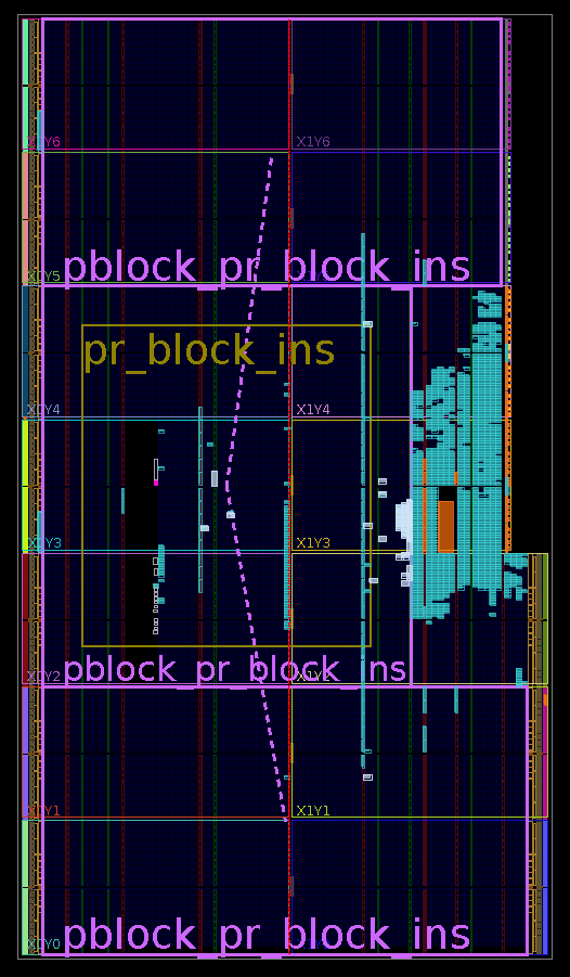
Note that only slices, RAMs and DSP48 are limited by constraints. These are the only types of logic that Partial Reconfiguration can control with series-7 FPGAs. Everything else, which is in practice anything but "pure logic" must belong to the static design.
With Ultrascale FPGAs and later, virtually any logic can be reloaded with Partial Reconfiguration.
There are additional restrictions on Pblocks, but there's no point repeating chapters 6-8 in UG909 here.
Anyhow, it's a good idea to open an implemented design, no matter of what, zoom in and out on the FPGA's view, and watch how the logic elements are organized in the FPGA. In particular note that there are columns of logic of the same type. Sometimes there are a few logic elements in the middle of the columns that break the uniformity (in particular special logic elements, such as the ICAP block, PCIe blocks etc.).
It's worth mentioning that the topic of Pblocks is not specific to Partial Reconfiguration. For example, everything that is said in this section also applies to using Pblocks for hierarchical design.
More on floorplanning
And here come a couple of counterintuitive facts: Even though the graphical representation of floorplanning consists of shapes that are drawn on the FPGA's map, it applies only to the types of logic that are controlled by its placement constraints. So if almost all slices of the FPGA are allocated for Partial Reconfiguration, islands of other logic elements that are completely surrounded by these slices may very well belong to static logic. For example, there is no problem whatsoever if the ICAP block itself is in the middle of a rectangle that is assigned for Partial Reconfiguration.
This isn't all that weird given that the Partial Reconfiguration bitstream is directed towards certain logic elements and leaves others intact. But what about routing? If an ICAP block is stuck in the middle of reconfigurable logic, how are the wires drawn to slices of static logic?
This leads us to the second counterintuitive fact: The routing for the static design uses resources inside the reconfigurable region. This routing remains stable throughout the Partial Reconfiguration process, or else it wouldn't be static logic. So inside the reconfigurable region, the routing for the reconfigurable logic changes, but the routing for the static logic remains unchanged. If there's anything that feels like magic about this whole topic, it's this little fact. It's also the reason why using a partial bitstream that isn't compatible with the static logic is likely to disrupt the FPGA completely.
The reverse is not true, of course: The reconfigurable logic uses no resources except for those explicitly listed as in the XDC example above. As for routing resources, nothing in the static region will change while a Partial Reconfiguration bitstream is loaded, so in that sense, reconfigurable logic never influences the static region. Well, that's almost true: If the shape of the reconfigurable region isn't a plain rectangle, Vivado may let routing get outside the reconfigurable region. This happens only on Ultrascale FPGAs, for the purpose of improving routing.
What should be clear at this point, is that the rules for drawing floorplanning are not simple. The good news is that Vivado produces fairly informative Critical Warnings in response to violation of the rules of floorplanning. Hence finding the suitable floorplan by trial and error is a reasonable way to work.
Parent implementations and Child implementations
Regarding the implementation of reconfigurable logic, it is important to keep in mind that every single path in the FPGA must achieve the timing constraints, and that must be true before and after the reconfigurable logic is loaded. Hence an implementation of the reconfigurable logic, that is separate from the static logic, is impossible. Rather, the implementation is always performed on the entire FPGA for each reconfigurable module. The timing constraints (as well as other constraints) are enforced on each implementation.
To clarify this point, let's return to the example with moduleA and moduleB from above. For this example, Vivado performs the implementation of the full design with moduleA included, and then does the same with moduleB. As a byproduct, there are regular bitstream files for each of these two options.
It's worth emphasizing: All implementations produce a full initial bitstream and also a partial bitstream. This is true for all implementations , no matter if they are Parent or Child. Hence when the FPGA powers up, it's possible to load it with any of these initial bitstreams.
In order to make it possible to move from moduleA to moduleB with Partial Reconfiguration, everything in the static partition must be exactly the same. This includes the logic itself, the placement and the routing. To achieve this, Vivado performs the implementation for one scenario (e.g. with moduleA) as the Parent Implementation. It then performs Child Implementations for all other scenarios (e.g. with moduleB). How this is done exactly is detailed in the last post in this series, but to make a long story short:
Vivado begins with running the Parent Implementation for moduleA as usual for a Hierarchical Design. This means that the synthesis of the static logic and the reconfigurable logic is done separately, and that the floorplanning constraints enforce the placements into separate sites on the FPGA. Other than these two differences, a regular implementation is performed. In particular, placement and routing is performed for optimal results on this specific scenario (even though the floorplanning constraints and the separate synthesis may result in suboptimal performance).
The next step is carrying out the Child Implementation for moduleB. There is no need for a synthesis of the static design, as this has already been done on behalf of the Parent Implementation. So a synthesis is carried out only on the reconfigurable logic.
The implementation is then carried out in the same way as the Parent Implementation, with one crucial difference: The place and route of all static logic is forced to be identical with the result of the Parent Implementation. Given this limitation, place and route of the reconfigurable logic is carried out for optimal results.
So the key to the relations between the Parent and Child is that a Child Implementation starts where the Parent Implementation ended, but replaces the reconfigurable logic with its own logic. The Child Implementation then continues as usual, but without touching anything in the area of the static logic.
Because all Child Implementations need to adapt themselves to the static logic's placements and routes, it might be harder to achieve the timing constraints, compared with the regular implementation of the design. There are in fact two obstacles:
- The hierarchical separation of the design into static logic and reconfigurable logic prevents optimization across their boundaries.
- The static logic's place and route is not necessarily optimal for the reconfigurable logic.
This should be kept in mind when choosing which of the reconfigurable modules should be chosen for the Parent Implementation. For example, it might be the module that is most difficult to achieve the timing constraints with. Or the module that represents the other modules in the way it connects with the static logic. Or possibly, the other way around: A reconfigurable module that effectively includes no logic at all (a "grey box"), in order to achieve a neutral implementation of the static logic.
As for the usage of the bitstreams, Vivado's paradigm for the implementation of a project with Partial Reconfiguration is that the implementation ends when all bitstreams are up-to-date and mutually compatible. In other words, any of the implementations' initial bitstreams can be used for loading the FPGA in the beginning. After this, any of the implementations' partial bitstreams can be loaded.
Hence the first "Generate Bitstream" starts the Parent Implementation and all Child Implementations. In compilations that follow, Vivado carries out only runs that need update, as usual.
The Dynamic Function eXchange Wizard
The purpose of this Wizard, which can be started from the Tools menu, is to define the Parent Implementation and Child Implementations, and in particular which Implementation contains which reconfigurable module.
It's easiest to explain this Wizard by looking at the Tcl commands it makes when adding a Child Implementation:
create_reconfig_module -name bpf -partition_def [get_partition_defs pr ]
add_files -norecurse /path/to/pr_block1.v  -of_objects [get_reconfig_modules bpf]
create_pr_configuration -name config_2 -partitions [list pr_block_ins:bpf ]
create_run child_0_impl_1 -parent_run impl_1 -pr_config config_2 -flow {Vivado Implementation 2020}
I'll go through this Tcl sequence backwards, from the last row to first:
So in the last row, a Child Implementation run is created. The new run is given the name "child_0_impl_1" and its parent run is chosen to be "impl_1". No less important, the configuration of this new run is set to be "config_2".
"config_2" is defined in the third row, saying that "bpf" is the reconfigurable module that intended for the reconfigurable partition that is named "pr_block_ins" . "pr_block_ins" has been mentioned above, but what is "bpf"?
In the first row, a reconfig_module is created and named "bpf" — this is just any name that is convenient for telling what the logic does. The second row says that a certain Verilog file is added to this reconfigurable module.
So all in all, these four rows create a new Child Implementation, and say that the synthesis of a certain Verilog file is required to create a reconfigurable module. Also, two objects in the Tcl environment are created, "bpf" and "config_2".
Now back to the Dynamic Function eXchange Wizard: It's a GUI tool, which represents the relations between design sources, reconfigurable modules, configurations and implementation runs. It's just a convenient way to communicate the information for producing Tcl commands like those shown above.
This tool may seem overly complicated, but that's because the example is simple. In a realistic design, it's likely that reconfig_module has several source files, and possibly IPs assigned to it. So the GUI makes things easier.
But why is the configuration ("config_2") necessary? Why isn't the connection between "bpf" and "pr_block_ins" made with the create_run command? Once again, that's a legitimate question because this post is restricted to only one reconfigurable partition. If there are several such partitions, a configuration defines which partition gets which reconfigurable module, so it makes sense to give each such combination a name, like config_*.
So if there are multiple partitions, is it required to make an implementation for each possible combination of reconfigurable modules? This question isn't relevant for this series of posts, so feel free to skip to the next section.
Recall that Vivado's implementation is made on the entire design, i.e. the static logic and reconfigurable logic together, and ensures that it meets timing constraints as a whole. Therefore, if there are multiple partitions, the safe way to use Partial Reconfiguration is to load all partitions with their partial bitstreams, so that all partial bitstreams are the result of the same implementation run. In other words, all partial bitstreams were created with the same configuration (e.g. "config_2"), and therefore the combination of these partial bitstreams is the result of an implementation that has been validated by the tools. In particular, this implementation is known to achieve the timing constraints.
And yet, if the reconfigurable modules have no mutual interaction (i.e. all the top-level ports of reconfigurable modules are connected to static logic, and not to each other), I can't figure out what could go wrong with treating each partition separately. Indeed, Vivado hasn't explicitly approved timing of the FPGA as a whole if partial bitstreams from different runs are used in mixture. But since all paths with the static logic have achieved the timing constraints, and the static logic is exactly the same on all implementation runs, isn't that good enough? The official documentation doesn't seem to give information on this issue.
Routing and Partition Pins
There's still one piece missing in the puzzle: The routing that connects between the static logic and the reconfigurable logic. Recall that the Parent Implementation does the place and route of the design in the optimal way for the reconfigurable logic that is included in the relevant configuration. But then the child's reconfigurable module needs to fit into the same reconfigurable partition, and connect with the static design. At least some part of the routing belongs to the static logic, and can therefore not change.
This is where Partition Pins come in. Conceptually, one can think about the reconfigurable logic as a physical component, and the partition pins as the metal pins that connected to the PCB.
However in reality, partition pins are just positions in the coordinate system of the FPGA's resources for routing. They are the places where the static logic's routing ends, and the reconfigurable logic's routing continues. Their only importance is that the Parent Implementation and the Child Implementations agree on where they are.
No physical resources such as LUTs or flip-flops are required to establish these anchor points, and they don't contribute additional routing delay. The segment of routing that leads to and from the partition pins creates a delay, of course, but the partition pins themselves don't add any delay.
The positions of the partition pins are chosen by the tools automatically while the Parent implementation is carried out, and Child implementations are forced to adapt themselves. In other words, the routing between the static logic and reconfigurable logic starts where the Parent Implementation said it will, and the Child Implementation can only try its best inside the reconfigurable partition. It may turn out that some partition pins are placed in unfavorable positions for the Child's reconfigurable logic, which might cause difficulties in achieving the timing constraints.
Partition pins are often grouped together somewhere close to the reconfigurable partition's perimeter. It seems like Vivado is designed to select sites that aren't too specialized for a particular design.
However, partition pins can be found anywhere inside the reconfigurable partition, if that was necessary to achieve timing constraints during the Parent Implementation. Recall that the static design is allowed to use resources for routing that are inside the reconfigurable partition. Hence there's no problem that some of the static routing's segment goes into the reconfigurable partition.
To prevent problems with timing constraints and partition pins, it's beneficial if the output ports of the reconfigurable module are registers, and that the inputs are sampled by registers as well. Likewise, the static logic is better off applying registers similarly. In fact, it's always a good idea to follow this rule, whenever possible and when that doesn't complicate the design.
The Greybox
One more thing about the DFX Wizard is the greybox: In the Edit Configuration window, it's possible to assign a greybox as the reconfigurable module, instead of one of the regular reconfigurable modules. A greybox is a bogus module that is generated by Vivado. It fits the ports of the real reconfigurable module, but instead of real logic, there's one LUT for every port pin. The LUTs that are generated for inputs are connected to nothing on the other end, and the LUTs for outputs produce a zero value. For vector ports, a LUT is created for each bit in the vector.
It's may not be a good idea to use a greybox in the Parent Implementation, as it makes it too easy for place and route process. Even if the reconfigurable modules are very different from each other, it's probably better to write a simple module that challenges the tools to some extent.
But for the sake of creating an initial bitstream file with minimal logic, a child implementation that contains only greybox modules may be useful. Recall that all implementations produce complete bitstreams, that can all be used as the initial bitstream, since they all have the exact same static logic.
Clearing Bitstreams (Ultrascale only)
This relates only to Ultrascale FPGAs (not Ultrascale+).
As mentioned above, all implementations create two bitstreams: One bitstream for the entire design, which can be used to load the FPGA initially, with the related reconfigurable module included. The second bitstream is for Partial Reconfiguration with the same reconfigurable module.
With Ultrascale devices, there's a third bitstream, the "clearing bitstream", which is created on each implementation. This bitstream needs to be sent to the FPGA before the partial bitstream. Note that the clearing bitstream that is sent to the FPGA must match the logic that is currently inside the FPGA, and not the bitstream that is about to be loaded. Hence there's a need to keep track of the FPGA's current situation, something that is not necessary with other FPGA families.
Loading the clearing bitstream shuts down the reconfigurable module, even though it doesn't really change the logic. The output ports of this module may show any value until a new partial bitstream has been loaded and started.
According to UG909, loading the clearing bitstream of the wrong reconfigurable module (i.e. not the clearing bitstream that matches the logic that is already in the FPGA) may disrupt the static logic as well, and hence cause a malfunctions of the the reconfiguration mechanism.
Xilinx' documentation seems to be vague regarding what happens if a partial bitstream is loaded without loading the clearing bitstream first. In chapter 9 of UG909 it first says: "Prior to loading in a partial bitstream for a new Reconfigurable Module, the existing Reconfigurable Module must be cleared". So the conclusion would be that the clearing bitstream is mandatory.
But a few rows below, the same guide says "If a clearing bit file is not loaded, initialization routines (GSR) have no effect". This implies that it's OK not to use clearing bitstream at all, if it's OK that all synchronous elements (RAMs and flip-flops, in principle) wake up in an unknown state. In my own anecdotal experiments with skipping the clearing bitstream I saw no problems, but that proves nothing.
So with Ultrascale FPGAs, there's definitely a need to keep track of what's loaded in the FPGA. This can be done, for example, by adding an output port to the reconfigurable module, which has a constant value (an ID code) that is different for each reconfigurable module. This allows the static logic to identify which reconfigurable module is currently loaded. An ID code like this can be a good idea regardless.
Plugin vs. Remote Update use cases
This parent-child methodology, which Vivado has adopted, is apparently designed for a specific use case, that I'll call the plugin usage: Reducing the FPGA's cost by loading the reconfigurable module that is currently required, rather than having all possible functionalities inside the FPGA all the time. For example, if the FPGA is used to implement several image filters, Partial Reconfiguration allows to implement each filter as a reconfigurable module, and reload the FPGA only with the filter that is needed.
Xilinx uses the term "Dynamic Function eXchange" (DFX) for Partial Configuration, with seems to reflect the primary intended use of this technique.
The parent-child method works well When this is the purpose of Partial Reconfiguration. A complete kit of bitstream files is generated. Any of the initial bitstreams can be used to initialize the FPGA, and all reconfigurable bitstreams can be used later for Partial Reconfiguration. When a new version of the project is released, the entire kit, which consists of all bitfiles, is replaced.
But there's another usage pattern, which I shall refer to as Remote Update. It's when Partial Reconfiguration is used as a means for version upgrades, possibly in the far future. In this usage scenario, the initial bitstream is released at some point in time, and can't be changed afterwards. Later on, partial bitstreams are released, and these must be compatible with the initial bitstream. These later releases may go on for several years.
For Remote Update, the parent-child method may be hard to work with as is. Even though the it's possible to run the Child Implementation to obtain a new partial bitstream without a repeated Implementation of the parent, it can be difficult to do this for a long time. For example, an accidental change in the source code of the static logic invalidates the parent's design, which causes a repeated Parent Implementation. As a result, the new static logic is incompatible with the previous one, and hence the partial bitstream that are based upon it can't be used with the original initial bitstream.
So if Partial Reconfiguration is intended as a method to successively update the FPGA design over time, the implementation procedure needs some manipulation. This topic is discussed in the the last post in this series.
Compressing bitstreams
This isn't directly related to Partial Reconfiguration, but it's sometimes desired to have a small initial bitstream file, in particular for ensuring a quick start of the FPGA. In this context, Partial Reconfiguration becomes a means to finish the bringup process after a quick start. This can be done from the same data source (e.g. the SPI flash) or from a completely different one (e.g. a PCIe interface).
Compressing the bitstream is allowed for both the initial bitstream and the partial bitstreams.
This is the row to add to the XDC file to in order to request a compressed bitstream:
set_property bitstream.general.compress true [current_design]
This concludes the theoretical part. The next post shows the practical steps for configuring a project to use Partial Reconfiguration.