This web page belongs to a group of small projects that explore the features of the Smart Zynq board.
This project is also published in HelloFPGA, which is recommended for Chinese readers.
Introduction
This tutorial explains how to connect regular headphones to the Smart Zynq board and listen to music. The purpose of this project is to demonstrate the use of a Xillybus stream for the purpose of sending continuous data to the FPGA. The Verilog code that implements a PWM modulator is also shown here.
The code that is shown here is not an example for how to implement an audio output. The usual method for implementing an analog output is a more complicated technique, which is called Sigma-Delta. This technique can be implemented on an FPGA, however the theoretical background is much more difficult to understand.
Another drawback of this implementation is that its sample rate is inaccurate (48828 Hz instead of 48000 Hz). This can be fixed easily by changing the frequency of the clock that is used by the logic. The topic of manipulating the clocks for this purpose is not shown here, as this example focuses on simplicity rather than accuracy.
The equipment for this demonstration is:
- A Smart Zynq board (SP or SL).
- A pair of regular analog headphones.
- Crocodile clips and wires, or other means for connecting to the board's pins.
- Optional: A 50Ω-200Ω resistor. The purpose of this resistor is protect the headphones and the Smart Zynq board from an excessive electrical current. The example will work without this resistor, but with a risk for damage to the electronics.
Preparing the Vivado project
Create a new Vivado project from the demo bundle's zip file (the boot partition kit). Open verilog/src/xillydemo.v in a text editor. Delete the part of the code that is labeled "PART 2". Instead of that, insert this code snippet:
   /*
    * PART 2
    * ======
    *
    * This code demonstrates a PWM-based audio output
    */

   reg [10:0]   pwm_level, threshold_left, threshold_right;
   reg 		pwm_left, pwm_right;
   reg 		fifo_out_valid;
   wire [31:0] 	fifo_out;
   wire 	fifo_empty;

   wire 	fifo_rd_en = !fifo_out_valid && !fifo_empty;
   wire 	next_word = (pwm_level == 11'h7ff);

   assign J6 = { pwm_right, pwm_left };

   always @(posedge bus_clk)
     begin
	pwm_level <= pwm_level + 1;

	if (next_word && fifo_out_valid)
	  begin
	     // The audio samples are signed integers. Change them to
	     // unsigned by adding 1024.
	     threshold_left <= fifo_out[15:5] + 1024;
	     threshold_right <= fifo_out[31:21] + 1024;
	  end
	else if (next_word) // FIFO's output not valid, keep silent
	  begin
	     threshold_left <= 0;
	     threshold_right <= 0;
	  end

	pwm_left <= (threshold_left > pwm_level);
	pwm_right <= (threshold_right > pwm_level);

	if (fifo_rd_en)
	  fifo_out_valid <= 1;
	else if (next_word)
	  fifo_out_valid <= 0;
     end

   // 32-bit FIFO for audio samples
   fifo_32x512 fifo_32
     (
      .clk(bus_clk),
      // Interface with Xillybus IP core
      .srst(!user_w_write_32_open),
      .din(user_w_write_32_data),
      .wr_en(user_w_write_32_wren),
      .full(user_w_write_32_full),

      // Interface with application logic
      .rd_en(fifo_rd_en),
      .dout(fifo_out),
      .empty(fifo_empty)
      );

   // Send the text "PWM" to reassure that the correct bitstream is used.
   assign user_r_read_32_eof = 0;
   assign user_r_read_32_empty = 0;
   assign user_r_read_32_data = 32'h0a_4d_57_50; // "PWM" + LF
Alternatively, download the xillydemo.v file from here.
Create a bitstream file from the updated project in the same way that you created the bitstream file for the demo bundle. Also copy the bitstream file to the TF card in the same way (overwrite the old xillydemo.bit file with the file that was created with this project).
Connecting the headphones
Connect a 50Ω-200Ω resistor to the I/O pin that carries the audio signal: J6/1 (left ear) or J6/2 (right ear). In order to find J6, look for where it's written "Bank 33 VCCIO Vadj" at the back side of the Smart Zynq board. The row of pins that is close to this marking is the pin header that we shall work with. J6/1 is hence the pin that is closest to the HDMI connector.
Connect the other side of the resistor to the tip of the headphone plug. A crocodile clip can be used for this purpose.
Connect the headphone plug's sleeve part to Smart Zynq's ground. The pin header's ground is positioned at J6/35 or J6/36. However it is not recommended to use these pins, because they are near to power supply pins.
Instead, it's possible to use any pin in the range from J6/3 to J6/34 as well. The FPGA considers these as output pins, and maintains them at a '0' logic level. It's therefore possible to use these pins as ground.
It's also possible to obtain the connection to ground by connecting a crocodile clip to the outer metal part of one of the board's connectors: The Ethernet connector, the HDMI connector, or one of the USB connectors.
Start the board
Power on the Smart Zynq as usual (or perform a reboot). The next step is to ensure that the correct bitstream file is loaded into the FPGA (PL part).
Type the command "head /dev/xillybus_read_32" at shell prompt. This command reads the first rows from /dev/xillybus_read_32 and prints out the result:
# head /dev/xillybus_read_32
PWM
PWM
PWM
PWM
PWM
PWM
PWM
PWM
PWM
PWM
If there is no output from this command, or if the output is different from the one shown above, the incorrect bitstream is in use.
Playing an audio file
Copy an audio file to Xillinux' file system. In other words, the audio file should be available for commands inside the Linux system.
This file should be in WAV format: Uncompressed PCM, 2 channels, s16le (this is almost always the format of WAV files). The sampling rate should be 48000 Hz, but 44100 Hz will also work fairly well.
An adequate audio file can be downloaded from this link.
There are several methods to copy a file to a Linux system. For example, it's possible to use the Ethernet network to copy the file from another computer to Xillinux' home directory with this command:
$ scp sample.wav root@192.168.1.10:~/
This works with Microsoft Windows' command prompt as well as with a Linux shell. Change the IP address (192.168.1.10 in this example) to the board's IP address.
There are other methods to copy a file to Xillinux as well. For example, using NFS or CIFS.
Once the file is copied to Xillinux' file system, use this command to play the audio:
# cat sample.wav > /dev/xillybus_write_32
Replace "sample.wav" with the name of the file that you want to play. The command that is shown here works if the file is in the current directory.
The command plays the file on the headphones until a new shell prompt appears. You should be able to hear the music in one ear (or both ears, if you connected both J6/1 and J6/2 to separate parts of the headphones' plug).
It's possible to stop this command in the middle with CTRL-C.
That's it. The rest of this page explains how this works.
How the audio data reaches the FPGA
The "cat" command copies the content of the audio file (sample.wav) into a device file that is named "xillybus_write_32". In Linux systems, this is the usual method to send data to a hardware driver. In this example, the driver interfaces with Xillybus' IP core. As a result, the data is sent to a FIFO inside the FPGA's logic.
Let's look at the relevant part in the Verilog code that was presented above:
   fifo_32x512 fifo_32
     (
      .clk(bus_clk),
      // Interface with Xillybus IP core
      .srst(!user_w_write_32_open),
      .din(user_w_write_32_data),
      .wr_en(user_w_write_32_wren),
      .full(user_w_write_32_full),

      // Interface with application logic
      .rd_en(fifo_rd_en),
      .dout(fifo_out),
      .empty(fifo_empty)
      );
This is an instantiation of a standard FIFO. For a general explanation about how a FIFO works, please refer to this page.
This FIFO has three ports that are related to inserting data into the FIFO: din, wr_en and full. All three of these ports are connected to the Xillybus IP core. In other words, the three signals (user_w_write_32_data, user_w_write_32_wren and user_w_write_32_full) are connected to a module that is named xillybus. This arrangement allows the Xillybus IP core to write data into the FIFO.
Xillybus uses this arrangement to fill the FIFO with the data that the software writes to /dev/xillybus_write_32. Xillybus continuously attempts to write as much data as possible into the FIFO, but it never causes an overflow (i.e. it obeys the FIFO's full signal).
In summary, this is what happens:
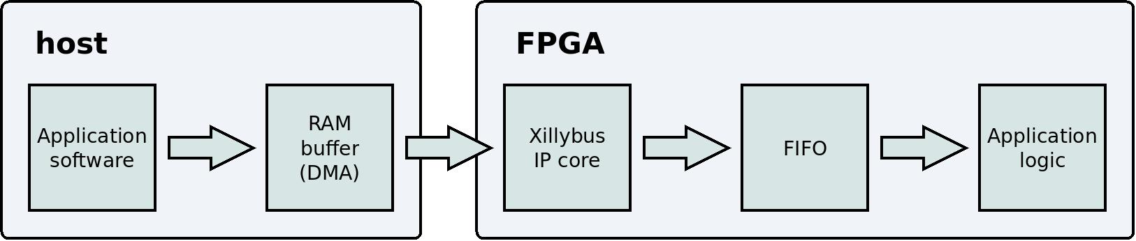
- The "cat" command copies the data from sample.wav to the device file. (/dev/xillybus_write_32).
- Xillybus' driver copies this data into a DMA buffer.
- Xillybus' logic inside the FPGA (the Xillybus IP core) reads the data from the DMA buffer and writes the data into the FIFO.
- The application logic inside the FPGA reads the data from the FIFO and consumes this data.
All these operations take place simultaneously and continuously.
For more information about Xillybus, refer to this series of pages, in particular this page.
How the audio signal is created
The description so far explained how the data reaches the application logic inside the FPGA. We shall now look at how the data turns into audio.
First, pay attention to this row in the Verilog code:
assign J6 = { pwm_right, pwm_left };
According to this, the two audio outputs consist of pwm_right and pwm_left. These two registers are assigned values as follows:
   always @(posedge bus_clk)
     begin
	pwm_level <= pwm_level + 1;

 [ ... ]
	pwm_left <= (threshold_left > pwm_level);
	pwm_right <= (threshold_right > pwm_level);
 [ ... ]
    end
Note that pwm_level is a simple counter. This register consists of 11 bits, so it counts from 0 to 2047, and then starts over from 0 again.
The value of pwm_left is '1' when threshold_left is larger than pwm_level. In other words, threshold_left is compared with a counter that repeatedly goes through all numbers from 0 to 2047. The higher value threshold_left has, the longer time will pwm_left have the value '1'. This is the principle of PWM: The pulse's length is linearly proportional to the value of the analog signal that we want to generate.
pwm_right works in the same way with relation to threshold_right.
threshold_left and threshold_right contain the data from the WAV file that is sent through the Xillybus IP core. We shall now look in detail how this happens.
First, let's look at the part in the FIFO's instantiation that is related to reading from the FIFO:
      // Interface with application logic
      .rd_en(fifo_rd_en),
      .dout(fifo_out),
      .empty(fifo_empty)
fifo_rd_en is defined as follows:
wire fifo_rd_en = !fifo_out_valid && !fifo_empty;
Hence the FIFO's read enable is high when the FIFO isn't empty and when fifo_out_valid is low. So let's look at the definition of fifo_out_valid:
   always @(posedge bus_clk)
     begin
 [ ... ]
	if (fifo_rd_en)
	  fifo_out_valid <= 1;
	else if (next_word)
	  fifo_out_valid <= 0;
     end
The meaning of fifo_out_valid is that this register is high when the output of the FIFO is valid. More precisely, fifo_out_valid is high when the FIFO's output has not been consumed yet. This is why this register changes to high one clock cycle after fifo_rd_en is high. This register changes to low when next_word is high. As we shall see below, the logic that implements the PWM consumes the FIFO's output when next_word is high.
next_word is defined as follows:
wire next_word = (pwm_level == 11'h7ff);
Recall that pwm_level is a counter that goes through all values between 0 and 2047. The hexadecimal coding for 2047 is 7ff. So next_word is high just before pwm_level is about to go back to zero.
How often is next_word high? The frequency of bus_clk is 100 MHz. next_word is high once for each round of 2048 clock cycles. 100 MHz ÷ 2048 ≈ 48828 Hz. So next_word is high around 48828 times per second.
I mentioned earlier that next_word is high when the FIFO's output is consumed. This is the relevant part in the Verilog code:
   always @(posedge bus_clk)
     begin
 [ ... ]

	if (next_word && fifo_out_valid)
	  begin
	     // The audio samples are signed integers. Change them to
	     // unsigned by adding 1024.
	     threshold_left <= fifo_out[15:5] + 1024;
	     threshold_right <= fifo_out[31:21] + 1024;
	  end
	else if (next_word) // FIFO's output not valid, keep silent
	  begin
	     threshold_left <= 0;
	     threshold_right <= 0;
	  end
 [ ... ]
    end
We shall first observe that when next_word is high, new values are assigned to both threshold_left and threshold_right. If fifo_out_valid is low, the value of these two registers becomes zero. This happens when no data is sent to the FIFO, so it becomes empty.
If fifo_out_valid is high, it means that the FIFO's dout port contains the value of an audio sample. This value represents the analog signal of the two stereo channels. Each such sample contains two signed numbers that are given in 16-bit 2's complement format.
The audio sample that belong to the left stereo channel is given in fifo_out[15:0]. This is a signed number between -32768 and 32767. The five lower bits are removed, so the range of fifo_out[15:5] is between -1024 and 1023. The expression "fifo_out[15:5] + 1024" is therefore an unsigned number between 0 and 2047. This range of numbers is suitable for comparison with pwm_level.
Accordingly, when fifo_out[15:0] equals -32768, threshold_left will be assigned the value zero. The condition "threshold_left > pwm_level" is never met, so pwm_left remains low all the time. On the other hand, when fifo_out[15:0] equals 32767, threshold_left's value is 2047. As a result, pwm_left is high almost all the time. This is how fifo_out[15:0] controls how long time pwm_left is high on each pulse. fifo_out[31:16] controls pwm_right in the same way.
To summarize the entire mechanism: next_word is high once in every 2047 clock cycles. When next_word is high, the output of the FIFO is adjusted and copied into threshold_left and threshold_right. This consumes the FIFO's output, so fifo_out_valid becomes low. Consequently, if the FIFO is not empty, fifo_rd_en becomes high in order to read a new audio sample from the FIFO.
Recall that the Xillybus IP core fills this FIFO with the content of sample.wav. So there is a data flow of audio samples from the content of sample.wav to threshold_left and threshold_right. As mentioned above, next_word is high around 48828 times per second. This is the sample rate of this mechanism.
threshold_left controls the proportion of time that pwm_left is high. The same goes with regards to threshold_right and pwm_right. And finally, pwm_right and pwm_left are connected to the output port named J6, so these are the signals that are visible on the pin header.
Note that when next_word is high, two things happen: An audio sample is consumed, and pwm_level begins counting from zero. Hence one pulse is generated for each audio sample.
Printing out "PWM"
Earlier, I encouraged you to use the command "head /dev/xillybus_read_32" in order to ensure that the FPGA contains the correct bitstream. The expected result was that "PWM" is printed out many times. This is implemented by this part in the Verilog code:
   // Send the text "PWM" to reassure that the correct bitstream is used.
   assign user_r_read_32_eof = 0;
   assign user_r_read_32_empty = 0;
   assign user_r_read_32_data = 32'h0a_4d_57_50; // "PWM" + LF
If you look at xillydemo.v like it was before making the changes, you will see that user_r_read_32_rden, user_r_read_32_data and user_r_read_32_empty were connected to the FIFO. The Xillybus IP core uses these signals to read data from a FIFO and make this data available as a stream of data that is presented with /dev/xillybus_read_32.
Before the change in xillydemo.v, these signals were connected to the same FIFO that the Xillybus IP core writes to. The result was a loopback: The data that was written to /dev/xillybus_write_32 by the software was first inserted into the FIFO by the Xillybus IP core. The Xillybus IP core then read the data from the FIFO and presented it with /dev/xillybus_read_32. The purpose of this loopback is to be a starting point for learning how Xillybus works.
After the change in xillydemo.v, these signals are disconnected from the FIFO. Instead, user_r_read_32_data always equals 0x0a4d5750 and user_r_read_32_empty is always zero. Besides, user_r_read_32_rden is ignored by the logic. This creates an imaginary FIFO which is never empty. The output of this imaginary FIFO always has the same value: 0x0a4d5750. The Xillybus IP core behaves as if there was a FIFO that was always filled with this constant value. Therefore, when reading from /dev/xillybus_read_32, the word 0x0a4d5750 arrives repeatedly. When this word is printed out, it is interpreted as four bytes: 0x50, 0x57, 0x4d and 0x0a. In other words, the characters P, W, M and a line feed (which is used to mark the end of a row in Linux).
The relation between Verilog code and real pins
The Verilog code above connects the PWM signals to J6, but how does this reach the pin header? The answer can be found in xillydemo.xdc. This file is part of the Vivado project that creates the bitstream (in the "vivado-essentials" directory).
xillydemo.xdc contains various information that is necessary for the FPGA to work properly as an electronic component. Among others, this file contains these rows:
[ ... ]

## J6 on board (BANK33 VADJ)
set_property PACKAGE_PIN U22  [get_ports {J6[0]}];   #J6/1  = IO_B33_LN2
set_property PACKAGE_PIN T22  [get_ports {J6[1]}];   #J6/2  = IO_B33_LP2
set_property PACKAGE_PIN W22  [get_ports {J6[2]}];   #J6/3  = IO_B33_LN3
set_property PACKAGE_PIN V22  [get_ports {J6[3]}];   #J6/4  = IO_B33_LP3
set_property PACKAGE_PIN Y21  [get_ports {J6[4]}];   #J6/5  = IO_B33_LN9
set_property PACKAGE_PIN Y20  [get_ports {J6[5]}];   #J6/6  = IO_B33_LP9
set_property PACKAGE_PIN AB22 [get_ports {J6[6]}];   #J6/7  = IO_B33_LN7
set_property PACKAGE_PIN AA22 [get_ports {J6[7]}];   #J6/8  = IO_B33_LP7

[ ... ]
The first row says that the signal J6[0] should be connected to U22. This is a position on the FPGA's physical package. According to Smart Zynq's schematics, this FPGA pin is connected to the first pin of the pin header. The positions of the other ports are defined in the same manner.
I mentioned above that any pin in the range from J6/3 to J6/34 can be used as a ground, because these output pins have the value '0'. This is true because J6 consists of 34 bits, according to this row at the beginning of xillydemo.v:
inout [33:0] J6, //BANK33 VADJ
Recall that the value assignment of J6 is as follows:
assign J6 = { pwm_right, pwm_left };
This means that J6[0] equals pwm_left and J6[1] equals pwm_right. What about the rest? According to Verilog's syntax, all other bits are assigned the value zero.
The DC bias
The pin header is connected to the FPGA's logic outputs. Each of these pins have a voltage around 3.3V when the logic state is '1'. When the logic state is '0', the voltage is around 0V.
If the value of the original audio sample is zero, the values of threshold_left and threshold_right will be 1024. In other words, pwm_right and pwm_left will be high during half of the time, on the average. The average voltage (DC) is hence 3.3V ÷ 2 = 1.65V. So even if the audio samples in the WAV file have a perfect DC balance, the headphones are exposed to 1.65V as a DC component.
The purpose of the 100Ω resistor is hence not only to reduce the sound level, but to restrict the DC current. But even without this resistor, the electrical current will probably be harmless because of the FPGA's own limit and the headphone's electrical resistance. The resistor is merely a precaution measure.
Summary
This project showed how to use a digital output pin for the purpose of producing an analog audio signal that can be connected directly to headphones. The emphasis in this project was to present the use of a Xillybus stream for the purpose of sending data from software to the FPGA. A simple implementation of a PWM was also shown.