通常我更喜欢通过确保将所有寄存器放入 I/O 单元来处理 I/O 时序。时序(timing)很重要。
I/O register packing 似乎不是 Quartus的默认设置。无论如何,这是懒人应对这种情况的秘诀。
在这篇文章的前一个版本中,我建议在所有 I/Os上禁用时序 checking (timing checking)。这会在实现(implementation)期间使 unconstrained path warning 静音,特别是它可以防止 Quartus报告窗格中的“TimeQuest Timing Analyzer”部分变红:
set_false_path -from [get_ports]
set_false_path -to [get_ports]
事实证明,这不是一个好主意,尤其是关于输入端口。这将在下面进一步详述。
然而,需要说服 fitter 将寄存器放入 I/O block。在 QSF中,添加
set_instance_assignment -name FAST_OUTPUT_REGISTER ON -to *
set_instance_assignment -name FAST_INPUT_REGISTER ON -to *
set_instance_assignment -name FAST_OUTPUT_ENABLE_REGISTER ON -to *
绝对在每个寄存器(register)上制作这些 assignments 有点激进,但它确实完成了工作。 fitter 为 I/O elements 发出 warnings ,它未能强制执行这些约束(constraints),这实际上是一件好事。
要查看它的运行情况,请查看 fitter 报告的“资源 Section(Resource Section)”(可能在 Quartus的报告 pane(reports pane)中找到它)并寻找“输入寄存器(Input Registers)”等,无论适用。
在涉及 I/O cells的路径(paths)的时序报告(timing reports)中,差异很明显。例如,比较这个涉及 I/O 寄存器的路径:
+----------------------------------------------------------------------------------+
; Data Arrival Path                                                                ;
+---------+---------+----+------+--------+-----------------------+-----------------+
; Total   ; Incr    ; RF ; Type ; Fanout ; Location              ; Element         ;
+---------+---------+----+------+--------+-----------------------+-----------------+
; 2.918   ; 2.918   ;    ;      ;        ;                       ; data path       ;
;   0.000 ;   0.000 ;    ;      ; 1      ; DDIOOUTCELL_X3_Y0_N32 ; rst             ;
;   0.465 ;   0.465 ; RR ; CELL ; 1      ; DDIOOUTCELL_X3_Y0_N32 ; rst|q           ;
;   0.465 ;   0.000 ; RR ; IC   ; 1      ; IOOBUF_X3_Y0_N30      ; RESETB~output|i ;
;   2.918 ;   2.453 ; RR ; CELL ; 1      ; IOOBUF_X3_Y0_N30      ; RESETB~output|o ;
;   2.918 ;   0.000 ; RR ; CELL ; 0      ; PIN_P3                ; RESETB          ;
+---------+---------+----+------+--------+-----------------------+-----------------+
请注意 DDIOOUTCELL 元素,以及寄存器和 IOOBUF之间的布线(routing)中的 zero increment 。
作为比较,这里有一条路径(path)没有应用 I/O 寄存器(因为它被逻辑阻止了):
+--------------------------------------------------------------------------------+
; Data Arrival Path                                                              ;
+---------+---------+----+------+--------+-----------------+---------------------+
; Total   ; Incr    ; RF ; Type ; Fanout ; Location        ; Element             ;
+---------+---------+----+------+--------+-----------------+---------------------+
; 8.284   ; 8.284   ;    ;      ;        ;                 ; data path           ;
;   0.000 ;   0.000 ;    ;      ; 1      ; FF_X3_Y0_N17    ; Dir_flop_sig        ;
;   0.496 ;   0.496 ; RR ; CELL ; 8      ; FF_X3_Y0_N17    ; Dir_flop_sig|q      ;
;   2.153 ;   1.657 ; RR ; IC   ; 1      ; IOOBUF_X3_Y0_N9 ; DATA[7]~output|oe   ;
;   8.284 ;   6.131 ; RF ; CELL ; 1      ; IOOBUF_X3_Y0_N9 ; DATA[7]~output|o    ;
;   8.284 ;   0.000 ; FF ; CELL ; 1      ; PIN_T3          ; DATA[7]             ;
+---------+---------+----+------+--------+-----------------+---------------------+
在这里,我们看到通用触发器(flip-flop)如何生成信号,导致布线时延(routing delay)相当于 1.657 ns。主要问题是每个实现(implementation)的布线时延都不同,所以如果主板有信号 integrity (signal integrity)问题, FPGA 可能会受到指责,因为不同的 FPGA 设计版本似乎可以解决问题或使其重新出现。
时序约束(Timing constraints)
输入端口和输出端口(output ports)都应该有紧时序约束,所以除了充分利用 I/O 寄存器之外是无法满足的。如果所需的寄存器 packing(register packing)出现问题,这不仅会生成时序 failure (timing failure),而且还需要实现最小的 input-to-register 时序,如下所述。
以下讨论仅适用于驱动寄存器的时钟与外部时钟直接相关的情况(例如,通过锁相环(PLL)将时钟与某个整数相乘)。如果驱动寄存器的时钟与外部时钟实际上无关,情况会变得复杂得多,正如本文所述。
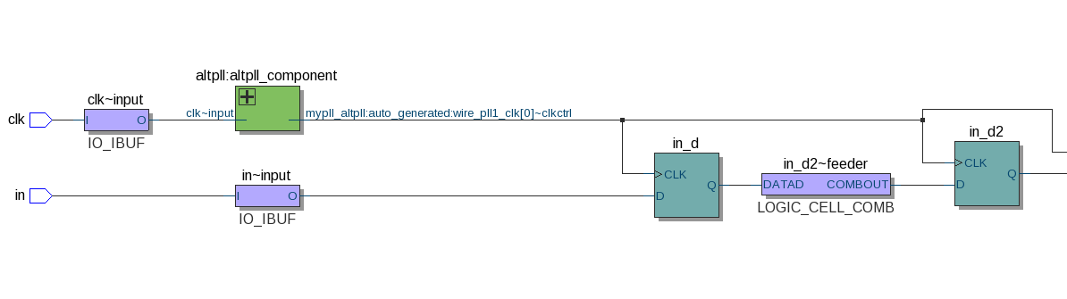
要演示此问题,请考虑以下 Verilog 代码:
module top
  (
   input        clk,
   input        in,
   output reg   out
   );

   reg 		in_d, in_d2;
   wire  	pll_clk;

   always @(posedge pll_clk)
     begin
	in_d <= in;
	in_d2 <= in_d;
	out <= in_d2;
     end

  /* Here comes an instantiation of a phase-compensating PLL, which
     doesn't change the frequency */
endmodule
还要考虑 SDC file中的以下约束:
create_clock -name main_clk -period 10 -waveform { 0 5 } [get_ports {clk}]

derive_pll_clocks
derive_clock_uncertainty

set_input_delay -clock main_clk -max 8.5 [get_ports in*]
set_input_delay -clock main_clk -min 0 [get_ports in*]
如本文所述, set_input_delay 是信号源的最大值时延(delay),范围从时钟到有效的逻辑状态。由于时钟的时间周期设置为 10 ns,将时延约束(delay constraint)设置为 8.5 ns 可以允许 1.5 ns 出现,直到下一个时钟到达(位于 10 ns)。换句话说, FPGA引脚上的 setup time 有一个约束(constraint)值,该值限制其不超过 1.5 ns。
请注意, set_max_delay 也可以用于此目的(在某些情况下,这是唯一的方法),如本文所述。
这次编译(compilation)(连同上面显示的 FAST_INPUT_REGISTER ON QSF 分配)在时序报告中产生以下段:
+----------------------------------------------------------------------------------+
; Data Arrival Path                                                                ;
+---------+---------+----+------+--------+-------------------+---------------------+
; Total   ; Incr    ; RF ; Type ; Fanout ; Location          ; Element             ;
+---------+---------+----+------+--------+-------------------+---------------------+
; 0.000   ; 0.000   ;    ;      ;        ;                   ; launch edge time    ;
; 0.000   ; 0.000   ;    ;      ;        ;                   ; clock path          ;
;   0.000 ;   0.000 ; R  ;      ;        ;                   ; clock network delay ;
; 8.500   ; 8.500   ; F  ; iExt ; 1      ; PIN_F2            ; in                  ;
; 9.550   ; 1.050   ;    ;      ;        ;                   ; data path           ;
;   8.500 ;   0.000 ; FF ; IC   ; 1      ; IOIBUF_X0_Y22_N15 ; in~input|i          ;
;   9.308 ;   0.808 ; FF ; CELL ; 1      ; IOIBUF_X0_Y22_N15 ; in~input|o          ;
;   9.308 ;   0.000 ; FF ; IC   ; 1      ; FF_X0_Y22_N17     ; in_d|d              ;
;   9.550 ;   0.242 ; FF ; CELL ; 1      ; FF_X0_Y22_N17     ; in_d                ;
+---------+---------+----+------+--------+-------------------+---------------------+
与输出寄存器(output register)的情况不同,列表中没有类型为“DDIOINCELL”的触发器,但有一些看起来像普通触发器的东西。但是,请注意,此触发器的接线有 zero 时延(标记为红色),这清楚地表明触发器和输入缓冲区已熔合在一起。
此输入的数据手册报告(datasheet report)表示:
+---------------------------------------------------------------------------------------------------+
; Setup Times                                                                                       ;
+-----------+------------+-------+-------+------------+---------------------------------------------+
; Data Port ; Clock Port ; Rise  ; Fall  ; Clock Edge ; Clock Reference                             ;
+-----------+------------+-------+-------+------------+---------------------------------------------+
; in        ; main_clk   ; 1.282 ; 1.461 ; Rise       ; altpll_component|auto_generated|pll1|clk[0] ;
+-----------+------------+-------+-------+------------+---------------------------------------------+

+-----------------------------------------------------------------------------------------------------+
; Hold Times                                                                                          ;
+-----------+------------+--------+--------+------------+---------------------------------------------+
; Data Port ; Clock Port ; Rise   ; Fall   ; Clock Edge ; Clock Reference                             ;
+-----------+------------+--------+--------+------------+---------------------------------------------+
; in        ; main_clk   ; -0.683 ; -0.862 ; Rise       ; altpll_component|auto_generated|pll1|clk[0] ;
+-----------+------------+--------+--------+------------+---------------------------------------------+
根据要求, FPGA 所需的 setup time 低于约束设置的 1.5 ns 限制。
现在让我们用 2 ns松开输入 setup delay (input setup delay),其余一切保持原样,重新运行编译(compilation):
set_input_delay -clock main_clk -max 6.5 [get_ports in*]
set_input_delay -clock main_clk -min 0 [get_ports in*]
时序报告中的部分现在显示:
+----------------------------------------------------------------------------------+
; Data Arrival Path                                                                ;
+---------+---------+----+------+--------+-------------------+---------------------+
; Total   ; Incr    ; RF ; Type ; Fanout ; Location          ; Element             ;
+---------+---------+----+------+--------+-------------------+---------------------+
; 0.000   ; 0.000   ;    ;      ;        ;                   ; launch edge time    ;
; 0.000   ; 0.000   ;    ;      ;        ;                   ; clock path          ;
;   0.000 ;   0.000 ; R  ;      ;        ;                   ; clock network delay ;
; 6.500   ; 6.500   ; F  ; iExt ; 1      ; PIN_F2            ; in                  ;
; 8.612   ; 2.112   ;    ;      ;        ;                   ; data path           ;
;   6.500 ;   0.000 ; FF ; IC   ; 1      ; IOIBUF_X0_Y22_N15 ; in~input|i          ;
;   7.308 ;   0.808 ; FF ; CELL ; 1      ; IOIBUF_X0_Y22_N15 ; in~input|o          ;
;   8.370 ;   1.062 ; FF ; IC   ; 1      ; FF_X0_Y22_N17     ; in_d|d              ;
;   8.612 ;   0.242 ; FF ; CELL ; 1      ; FF_X0_Y22_N17     ; in_d                ;
+---------+---------+----+------+--------+-------------------+---------------------+
嗯?互连突然上升到 1.062 ns?!请注意,寄存器的位置没有改变,因此毫无疑问 in_d 是 I/O 寄存器。那么这个延迟是从哪里来的呢?
要回答这个问题,需要仔细研究设计。完整的编译,选择工具 > Netlist Viewers > Technology Map Viewer (Post-Fitting)(Tools > Netlist Viewers > Technology Map Viewer (Post-Fitting))后,出现如下 diagram (部分如下图,点击放大):
右键单击 in_d (寄存器)并选择 Locate Note > Locate in Resource Property Editor 显示以下内容(点击放大):
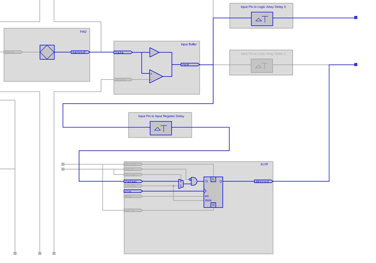
在此图的右侧(上面未显示),属性“输入 Pin to Input Register Delay(Input Pin to Input Register Delay)”设置为 2。这就是时延的原因。在约束松动之前,它被设置为 0。直接的教训是:
如果 setup 约束未设置为技术的最佳价值, Quartus 可能会增加时延的费用。
但是为什么, Quartus,为什么?
所以有人可能会奇怪为什么 Quartus 会在输入 pad (input pad)和寄存器之间插入这个时延(delay)。尽快取样不是重点吗?要回答这个问题,让我们看一下更新后的数据手册报告:
---------------------+
; Data Port ; Clock Port ; Rise  ; Fall  ; Clock Edge ; Clock Reference                             ;
+-----------+------------+-------+-------+------------+---------------------------------------------+
; in        ; main_clk   ; 2.205 ; 2.523 ; Rise       ; altpll_component|auto_generated|pll1|clk[0] ;
+-----------+------------+-------+-------+------------+---------------------------------------------+

+-----------------------------------------------------------------------------------------------------+
; Hold Times                                                                                          ;
+-----------+------------+--------+--------+------------+---------------------------------------------+
; Data Port ; Clock Port ; Rise   ; Fall   ; Clock Edge ; Clock Reference                             ;
+-----------+------------+--------+--------+------------+---------------------------------------------+
; in        ; main_clk   ; -1.570 ; -1.882 ; Rise       ; altpll_component|auto_generated|pll1|clk[0] ;
+-----------+------------+--------+--------+------------+---------------------------------------------+
回想一下, 2 ns 是从时延约束缩减而来的。因此,最大允许 setup time 从 1.5 ns 上升到 3.5 ns。很容易看出满足了这个要求, slack 几乎是 1 ns。
所以 Quartus 说“我可以轻松满足 setup 的要求,有多余的 2 ns。让我们给 setup time额外的 1 ns ,给 hold time requirement 额外的 1 ns (即 0 ns)”。事实上,通过在时延中添加 1.062 ns , hold time 从 -0.683 ns 改进到 -1.570 ns (请不要指责我为什么差异不准确)。
底线: Quartus 扩大了 setup 和 hold的余量,使输入对抖动(jitter)更加稳健。虽然这是一件相当明智的事情,但这通常是不希望发生的,也不期望发生。
结论: 如果你想从输入到寄存器获得绝对最小的时延,运行一次编译与一个失败的时延约束,然后松开约束刚好足以解决这个失败。这确保了 Quartus 不会为了更好的 hold time而添加这个输入时延(input delay)来尝试“改进”时序。
使用 DDR primitives
Intel的 FPGAs 在 I/O cells 上或附近有逻辑,专用于在双时钟 rate(clock rate)上产生输出以及对输入进行采样。此主题在相关用户指南 ug_altddio.pdf中有详细说明。实例化 DDR primitive (或使用 ALTDDIO_BIDIR megafunction)是强制工具将寄存器放入 I/O cells的一种有吸引力的方式。但是,这不一定是一个好主意。
例如,像这样的例化(instantiation):
altddio_bidir ioddr
 (
 .padio(pin),
 .aclr (1'b0),
 .datain_h(datain_h),
 .datain_l(datain_l),
 .inclock(clk),
 .oe(oe),
 .outclock(clk),
 .dataout_h(dataout_h),
 .dataout_l(dataout_l),
 .oe_out (),
 .aset (1'b0),
 .combout(),
 .dqsundelayedout(),
 .inclocken(1'b1),
 .outclocken(1'b1),
 .sclr(1'b0),
 .sset(1'b0));
 defparam
   ioddr.extend_oe_disable = "OFF",
   ioddr.implement_input_in_lcell = "OFF",
   ioddr.intended_device_family = "Cyclone IV E",
   ioddr.invert_output = "OFF",
   ioddr.lpm_hint = "UNUSED",
   ioddr.lpm_type = "altddio_bidir",
   ioddr.oe_reg = "REGISTERED",
   ioddr.power_up_high = "OFF",
   ioddr.width = 1;
这确实导致逻辑实现了双向 DDR 接口,但就时序而言,至少在 Cyclone IV上取得了部分成功。 clock-to-output 时序与封装在 I/O cell中的普通输出寄存器完全相同,但输入路径(input path)的延迟实际上与上面的例化相比更差。结果可能与其他 Intel FPGA 系列不同。
请注意,为了用 DDR primitive模仿普通的 SDR 寄存器,它的 datain_h 端口和 datain_l 端口必须连接到同一根电线,因此时钟的下降沿(falling edge)不会改变任何东西。同样,应该忽略 dataout_l 端口的值,因为它是在下降沿上采样的。另请注意,输出使能端口(output enable port)(oe) 是 SDR 输入— 据我所知,无法通过 DDR rate 和 Intel FPGAs打开和关闭 high-Z 。至少不使用提供的逻辑 primitives(logic primitives)。
现在来解释为什么它在输出寄存器上运行良好,而不是输入: 提示在上面的时序报告中: 即使对于普通的 I/O cell 寄存器, DDIOOUTCELL_Xn_Ym_Nk 组件也用作寄存器。换句话说, DDR output 寄存器甚至用于 single-rate 输出,但仅与一个时钟边沿(clock edge)一起使用。至于输入路径,上面的时序报告表明使用了逻辑阵列寄存器(logic fabric register)(FF_Xn_Ym_Nk)。这是症结所在: DDR input 逻辑也在逻辑阵列(logic fabric)中实现。更糟糕的是,在 DDR的情况下,组合 blocks (combinatorial blocks)被挤在 I/O cell 和触发器之间。坦率地说,我不明白为什么,因为每个这样的组合 block (combinatorial block)只是单个输入到单个输出之间的传递。
这些观察得到了时序报告以及 Quartus的 Post-Fit Technology Map Viewer显示的图纸的支持。尤其是那些无用的组合 blocks ,在这些信息源中更是一目了然。
整个问题很可能从一 FPGA family 到另一个不同。至于 Cyclone IV,只有将 DDR primitives 用于输出才有意义。
更重要的是,当需要输出寄存器时使用 DDR primitive 输出的事实允许生成与其他输出对齐的输出时钟(output clock)。为此,请分别在 datain_h 端口和 datain_l 端口上为 DDR output primitive 提供常数 '1' 和 '0' 。至于其他输出,则需要使用输出寄存器封装。因此,其他输出的切换与来自 DDR 输出的时钟的上升沿(rising edge)对齐。
嗯,差不多。输出时钟的时序分析(timing analysis)不同,因为时钟切换多路选择器(mux),选择两个输出寄存器(output registers)中的哪一个提供输出(水平滚动查看详细信息):
+------------------------------------------------------------------------------------------------------------------------------------+
; Data Arrival Path                                                                                                                  ;
+---------+---------+----+------+--------+-------------------------+-----------------------------------------------------------------+
; Total   ; Incr    ; RF ; Type ; Fanout ; Location                ; Element                                                         ;
+---------+---------+----+------+--------+-------------------------+-----------------------------------------------------------------+
; 0.000   ; 0.000   ;    ;      ;        ;                         ; launch edge time                                                ;
; 0.000   ; 0.000   ;    ;      ;        ;                         ; clock path                                                      ;
;   0.000 ;   0.000 ; R  ;      ;        ;                         ; clock network delay                                             ;
; 0.000   ; 0.000   ; R  ;      ; 1      ; PIN_B12                 ; osc_clock                                                       ;
; 5.610   ; 5.610   ;    ;      ;        ;                         ; data path                                                       ;
;   0.000 ;   0.000 ; RR ; IC   ; 1      ; IOIBUF_X19_Y29_N8       ; osc_clock~input|i                                               ;
;   0.667 ;   0.667 ; RR ; CELL ; 2      ; IOIBUF_X19_Y29_N8       ; osc_clock~input|o                                               ;
;   0.853 ;   0.186 ; RR ; IC   ; 1      ; CLKCTRL_G12             ; osc_clock~inputclkctrl|inclk[0]                                 ;
;   0.853 ;   0.000 ; RR ; CELL ; 165    ; CLKCTRL_G12             ; osc_clock~inputclkctrl|outclk                                   ;
;   1.971 ;   1.118 ; RR ; IC   ; 1      ; DDIOOUTCELL_X16_Y29_N11 ; sram_controller_ins|ddr_clk|auto_generated|ddio_outa[0]|muxsel  ;
;   3.137 ;   1.166 ; RR ; CELL ; 1      ; DDIOOUTCELL_X16_Y29_N11 ; sram_controller_ins|ddr_clk|auto_generated|ddio_outa[0]|dataout ;
;   3.137 ;   0.000 ; RR ; IC   ; 1      ; IOOBUF_X16_Y29_N9       ; sram_clk~output|i                                               ;
;   5.610 ;   2.473 ; RR ; CELL ; 1      ; IOOBUF_X16_Y29_N9       ; sram_clk~output|o                                               ;
;   5.610 ;   0.000 ; RR ; CELL ; 0      ; PIN_E10                 ; sram_clk                                                        ;
+---------+---------+----+------+--------+-------------------------+-----------------------------------------------------------------;
请注意,这不是 register-to-pin 分析,而是 clock-to-pin。不过, set_output_delay 约束将包含此路径。但是,从寄存器到端口的 set_max_delay 约束,如果使用的话,不会包含这条路径,所以需要单独处理。换句话说,如果使用 set_max_delay ,它必须是以下形式:
set_max_delay -from [get_clocks main_clk] -to [get_ports sram_clk] 3.8
现在,将此与另一个引脚与相同的电压标准(voltage standard)等进行比较,仅由寄存器驱动:
+----------------------------------------------------------------------------------------------------------------------+
; Data Arrival Path                                                                                                    ;
+---------+---------+----+------+--------+-------------------------+---------------------------------------------------+
; Total   ; Incr    ; RF ; Type ; Fanout ; Location                ; Element                                           ;
+---------+---------+----+------+--------+-------------------------+---------------------------------------------------+
; 0.000   ; 0.000   ;    ;      ;        ;                         ; launch edge time                                  ;
; 2.507   ; 2.507   ;    ;      ;        ;                         ; clock path                                        ;
;   0.000 ;   0.000 ;    ;      ;        ;                         ; source latency                                    ;
;   0.000 ;   0.000 ;    ;      ; 1      ; PIN_B12                 ; osc_clock                                         ;
;   0.000 ;   0.000 ; RR ; IC   ; 1      ; IOIBUF_X19_Y29_N8       ; osc_clock~input|i                                 ;
;   0.667 ;   0.667 ; RR ; CELL ; 2      ; IOIBUF_X19_Y29_N8       ; osc_clock~input|o                                 ;
;   0.853 ;   0.186 ; RR ; IC   ; 1      ; CLKCTRL_G12             ; osc_clock~inputclkctrl|inclk[0]                   ;
;   0.853 ;   0.000 ; RR ; CELL ; 165    ; CLKCTRL_G12             ; osc_clock~inputclkctrl|outclk                     ;
;   1.970 ;   1.117 ; RR ; IC   ; 1      ; DDIOOUTCELL_X37_Y29_N11 ; sram_controller_ins|dq_wr_data[6]|clk             ;
;   2.507 ;   0.537 ; RR ; CELL ; 1      ; DDIOOUTCELL_X37_Y29_N11 ; sram_controller:sram_controller_ins|dq_wr_data[6] ;
; 5.645   ; 3.138   ;    ;      ;        ;                         ; data path                                         ;
;   2.717 ;   0.210 ;    ; uTco ; 1      ; DDIOOUTCELL_X37_Y29_N11 ; sram_controller:sram_controller_ins|dq_wr_data[6] ;
;   3.182 ;   0.465 ; RR ; CELL ; 1      ; DDIOOUTCELL_X37_Y29_N11 ; sram_controller_ins|dq_wr_data[6]|q               ;
;   3.182 ;   0.000 ; RR ; IC   ; 1      ; IOOBUF_X37_Y29_N9       ; sram_dq[6]~output|i                               ;
;   5.645 ;   2.463 ; RR ; CELL ; 1      ; IOOBUF_X37_Y29_N9       ; sram_dq[6]~output|o                               ;
;   5.645 ;   0.000 ; RR ; CELL ; 1      ; PIN_G14                 ; sram_dq[6]                                        ;
+---------+---------+----+------+--------+-------------------------+---------------------------------------------------;
clock-to-output 的总时间相差不超过 35 ps,尽管后者的路径在表面上完全不同。这不是巧合。 FPGA 显然是为产生这种相似性而设计的。具体来说,上面的时序分析是 100°C温度下的 slow 1200 mV ,但这个微小的差异在其他分析条件下也是一致的。